


© janaka dharmasena dreamstime.com_technical
Application Notes |
The many uses of a 200 mA precision voltage reference
The LT6658 is not a run-of-the-mill reference or regulator, as it performs both functions equally well. Moreover, due to its unique architectural arrangement, it does much more than simply supply a precise voltage with plenty of current.
This is a product release announcement by Analog Devices Inc.. The issuer is solely responsible for its content.
The following circuits, which will be discussed throughout this article, demonstrate a wide range of circuit possibilities. While there are quite a few applications illustrated, there will undoubtedly be applications that LT6658 would make a compelling solution, but have not been explicitly implemented here. As a product that is both a voltage reference and regulator, LT6658 is referred to as the Refulator™.
The Refulator is intended for designs that require a precision reference and the ability to power associated signal chain components, such as data converters, amplifiers, bridge transducers, and other high performance circuit devices.
Introduction
This listing of key specifications and feature illustrates LT6658’s performance. Key reference specifications include drift at 10 ppm/°C and initial accuracy at 0.05%. Key regulator specifications are load regulation at 0.25 μV/mA with two outputs sourcing current at 150 mA and 50 mA. Outstanding PSRR, low noise, output tracking, and a noise reduction pin combine to bring together the best of both the reference and regulator worlds into a single package.
Dual Outputs:
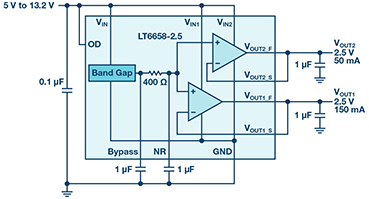 Figure 1. The LT6658 typical application.
The output buffers are trimmed to minimize drift resulting in excellent tracking over operating and load conditions. The complete data sheet with specifications can be found here.
Simple Output Configurations and Applications
Since the inverting inputs are available they can be arranged for nonunity gain, as shown in Figure 2. A LT5400-4 has 0.01% matching maintaining the precision of the LT6658. This example provides a precise 5 V and 2.5 V rail and can be used as a ±2.5 V regulator application with a split supply ground provided by the 2.5 V output. Nonunity gain can be applied to both outputs to generate any output voltage between 1 V and 6 V.
Figure 1. The LT6658 typical application.
The output buffers are trimmed to minimize drift resulting in excellent tracking over operating and load conditions. The complete data sheet with specifications can be found here.
Simple Output Configurations and Applications
Since the inverting inputs are available they can be arranged for nonunity gain, as shown in Figure 2. A LT5400-4 has 0.01% matching maintaining the precision of the LT6658. This example provides a precise 5 V and 2.5 V rail and can be used as a ±2.5 V regulator application with a split supply ground provided by the 2.5 V output. Nonunity gain can be applied to both outputs to generate any output voltage between 1 V and 6 V.
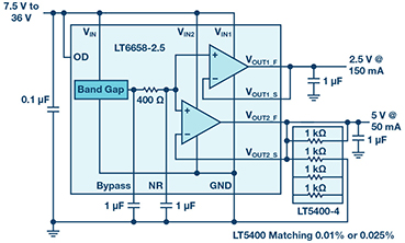 Figure 2. Simple, nonunity gain circuit creating a ±2.5 V split supply with ground.
A lower output voltage can be generated from a higher output voltage using the inverting input. Figure 3 demonstrates how a 3.3 V output can be used to generate a 1.8 V output. Since the noninverting inputs are tied to 2.5 V, it’s simple to create a lower output voltage. The expression for VOUT2_F is ___ where RF1 and RF2 are the buffer feedback resistors and RIN1 and RIN2 are the buffer input resistors.
Figure 2. Simple, nonunity gain circuit creating a ±2.5 V split supply with ground.
A lower output voltage can be generated from a higher output voltage using the inverting input. Figure 3 demonstrates how a 3.3 V output can be used to generate a 1.8 V output. Since the noninverting inputs are tied to 2.5 V, it’s simple to create a lower output voltage. The expression for VOUT2_F is ___ where RF1 and RF2 are the buffer feedback resistors and RIN1 and RIN2 are the buffer input resistors.
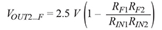
 Figure 3. An application with gain and inversion.
The only parameter that is compromised in this application is accuracy, which is dependent on the ratios of RF/RIN. In addition, this application illustrates how the BYPASS output can be used as a ±10 mA source and sink output. Note that any change on the BYPASS pin will directly affect the VOUT1 and VOUT2 outputs.
The output voltages can be trimmed to values between 2.5 V and 6 V, as shown in Figure 4. The trims can be accomplished with mechanical trim or digital trim pots. Digital trim is especially helpful to correct for ADC and DAC errors. The trim pots can be ganged to produce the same output voltage or the outputs voltages can be independently controlled.
Figure 3. An application with gain and inversion.
The only parameter that is compromised in this application is accuracy, which is dependent on the ratios of RF/RIN. In addition, this application illustrates how the BYPASS output can be used as a ±10 mA source and sink output. Note that any change on the BYPASS pin will directly affect the VOUT1 and VOUT2 outputs.
The output voltages can be trimmed to values between 2.5 V and 6 V, as shown in Figure 4. The trims can be accomplished with mechanical trim or digital trim pots. Digital trim is especially helpful to correct for ADC and DAC errors. The trim pots can be ganged to produce the same output voltage or the outputs voltages can be independently controlled.
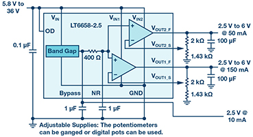 Figure 4. Adjustable gain.
Having two output buffers provides flexibility where one output can provide a necessary voltage, and the other output can provide a precision current source, as shown in Figure 5.
Note that the output VOUT2_F pin will be one VBE higher than the sense line. The supply voltage should be adjusted to accommodate the higher output voltage on VOUT2_F. Since each output has an independent supply input, they can be driven separately to improve channel-to-channel isolation or to accommodate different output voltages without consuming excessive power.
Figure 4. Adjustable gain.
Having two output buffers provides flexibility where one output can provide a necessary voltage, and the other output can provide a precision current source, as shown in Figure 5.
Note that the output VOUT2_F pin will be one VBE higher than the sense line. The supply voltage should be adjusted to accommodate the higher output voltage on VOUT2_F. Since each output has an independent supply input, they can be driven separately to improve channel-to-channel isolation or to accommodate different output voltages without consuming excessive power.
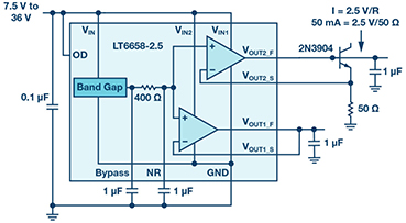 Figure 5. A precision voltage source and a precision current source application.
Typically, when one mentions a voltage reference and oscillation in the same sentence, they are referring to undesirable behavior. However, to highlight the unique architecture of the LT6658, the multivibrator circuit in Figure 6a is introduced, along with the resulting waveforms in Figure 6b. Here a 2.2 μF capacitor and 1 kΩ resistor set the time constant. The 400 Ω external positive feedback resistor and 400 Ω internal resistor set the hysteresis and affect the output frequency, which is roughly
f = 1/2.2 RC. The value of the internal resistor is 400 Ω ±15%, which will affect the output frequency.
Figure 5. A precision voltage source and a precision current source application.
Typically, when one mentions a voltage reference and oscillation in the same sentence, they are referring to undesirable behavior. However, to highlight the unique architecture of the LT6658, the multivibrator circuit in Figure 6a is introduced, along with the resulting waveforms in Figure 6b. Here a 2.2 μF capacitor and 1 kΩ resistor set the time constant. The 400 Ω external positive feedback resistor and 400 Ω internal resistor set the hysteresis and affect the output frequency, which is roughly
f = 1/2.2 RC. The value of the internal resistor is 400 Ω ±15%, which will affect the output frequency.
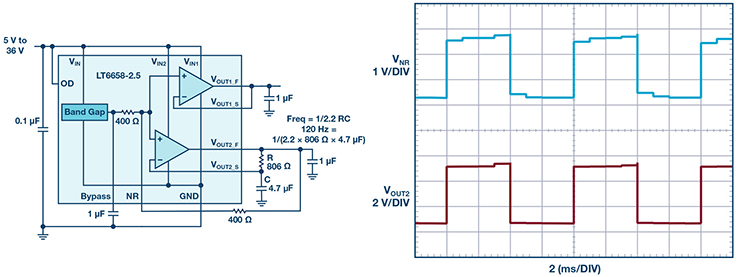 Figure 6a. Multivibrator application. / Figure 6b. Multivibrator output.
This circuit example shows the output voltage swing is slightly less than 4 V where the output low voltage goes down to 0.9 V and the output high voltage reaches to VIN – 2.5 V. VIN in this example is 6 V and the output is not fully loaded. As VIN increases past 8.5 V, the output will clamp around 6 V and the output duty cycle will reduce to about 40%.
Since current is flowing through the 400 Ω internal resistor, the voltage at the NR pin varies, causing VOUT1 to also oscillate synchronously with VOUT2.
Another dynamic circuit that is usually not associated with a voltage reference is the audio amplifier. The dual class A/B outputs can be arranged to drive 8 Ω and 16 Ω speakers, as shown in Figure 7. A single-ended source drives the inverting input of VOUT1, which drives the inverting input of VOUT2. The band gap sets a precision common mode, while the outputs act as a differential driver. To improve slew rate, use the minimum output capacitance on the LT6658.
Figure 6a. Multivibrator application. / Figure 6b. Multivibrator output.
This circuit example shows the output voltage swing is slightly less than 4 V where the output low voltage goes down to 0.9 V and the output high voltage reaches to VIN – 2.5 V. VIN in this example is 6 V and the output is not fully loaded. As VIN increases past 8.5 V, the output will clamp around 6 V and the output duty cycle will reduce to about 40%.
Since current is flowing through the 400 Ω internal resistor, the voltage at the NR pin varies, causing VOUT1 to also oscillate synchronously with VOUT2.
Another dynamic circuit that is usually not associated with a voltage reference is the audio amplifier. The dual class A/B outputs can be arranged to drive 8 Ω and 16 Ω speakers, as shown in Figure 7. A single-ended source drives the inverting input of VOUT1, which drives the inverting input of VOUT2. The band gap sets a precision common mode, while the outputs act as a differential driver. To improve slew rate, use the minimum output capacitance on the LT6658.
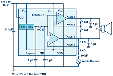 Figure 7. An audio application circuit.
With the addition of complementary discrete BJT output devices, the circuit in Figure 8 can supply more power. The circuit shows only one amplifier circuit, though two speakers can be driven by the two outputs to create stereo. While there are better audio amplifier choices, these applications demonstrate the flexibility of the LT6658 architecture.
Figure 7. An audio application circuit.
With the addition of complementary discrete BJT output devices, the circuit in Figure 8 can supply more power. The circuit shows only one amplifier circuit, though two speakers can be driven by the two outputs to create stereo. While there are better audio amplifier choices, these applications demonstrate the flexibility of the LT6658 architecture.
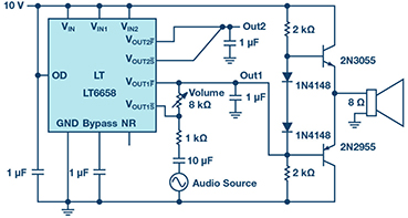 Figure 8. An audio application circuit using discrete BJTs.
Strain Gage Applications
The LT6658 can act as a regulator and a reference, as shown in the following strain gage application (Figure 9). The LT6658 provides the reference voltage and supply voltage to four LTC2440, and the 2.5 V rail biases the four strain gages. Each strain gage draws 7.5 mA totaling 30 mA, which is well within VOUT2’s 50 mA output specification and provides the ADC reference input. VOUT1 supplies 8 mA to each LTC2440 for a total of 32 mA.
Figure 8. An audio application circuit using discrete BJTs.
Strain Gage Applications
The LT6658 can act as a regulator and a reference, as shown in the following strain gage application (Figure 9). The LT6658 provides the reference voltage and supply voltage to four LTC2440, and the 2.5 V rail biases the four strain gages. Each strain gage draws 7.5 mA totaling 30 mA, which is well within VOUT2’s 50 mA output specification and provides the ADC reference input. VOUT1 supplies 8 mA to each LTC2440 for a total of 32 mA.
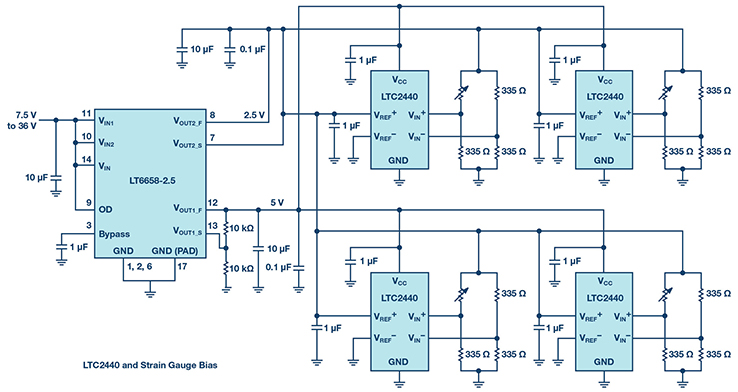 Figure 9. The LT6658 as a reference and regulator for a strain gage application.
Figure 10 shows a bridge circuit application with three load cells. The LT6658 provides a precise and stable operation even though the total load resistance is only 82 Ω requiring 60 mA. The high gain buffer will maintain a precise voltage capable of driving the load cells. The second output can drive another strain gage or supply power to the ADC converter downstream.
Figure 9. The LT6658 as a reference and regulator for a strain gage application.
Figure 10 shows a bridge circuit application with three load cells. The LT6658 provides a precise and stable operation even though the total load resistance is only 82 Ω requiring 60 mA. The high gain buffer will maintain a precise voltage capable of driving the load cells. The second output can drive another strain gage or supply power to the ADC converter downstream.
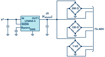 Figure 10. A bridge circuit application.
Data Acquisition Applications
For precision applications that use a DAC where the reference current is code dependent, it is important to pay special attention to board layout and parasitic resistance. To maintain an INL < 0.1 LSB with the LTC2641, load regulation needs to be <19 ppm/mA. Further, reference output impedance and PCB resistance needs to be <48 mW. The LT6658 has a dc output resistance of about 0.2 mW, leaving a 47.8 mW error budget for PCB resistance.
Figure 11 shows an application with two LTC2641 precision, 16-bit DACs. Since the reference current of the LTC2641 is code dependent, the two DAC reference inputs require a separate reference. The exception tracking of LT6658 output buffers translates into exceptional tracking of the DACs.
If only one DAC is required, the second output of the LT6658 can supply the input voltage to the DAC and other precision analog circuitry.
Figure 10. A bridge circuit application.
Data Acquisition Applications
For precision applications that use a DAC where the reference current is code dependent, it is important to pay special attention to board layout and parasitic resistance. To maintain an INL < 0.1 LSB with the LTC2641, load regulation needs to be <19 ppm/mA. Further, reference output impedance and PCB resistance needs to be <48 mW. The LT6658 has a dc output resistance of about 0.2 mW, leaving a 47.8 mW error budget for PCB resistance.
Figure 11 shows an application with two LTC2641 precision, 16-bit DACs. Since the reference current of the LTC2641 is code dependent, the two DAC reference inputs require a separate reference. The exception tracking of LT6658 output buffers translates into exceptional tracking of the DACs.
If only one DAC is required, the second output of the LT6658 can supply the input voltage to the DAC and other precision analog circuitry.
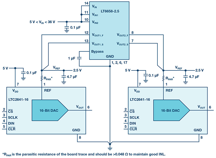 Figure 11. The LT6658 driving two code dependent DAC reference inputs.
The LTC2323-16 is a dual, 16-bit ADC with separate reference inputs. This allows for a different reference voltage for each ADC. Figure 12 shows one arrangement where 2.5 V and 5 V reference voltages drive the separate reference inputs. Again, the LT6658 output buffers track well maintaining conversion results that also track.
Figure 11. The LT6658 driving two code dependent DAC reference inputs.
The LTC2323-16 is a dual, 16-bit ADC with separate reference inputs. This allows for a different reference voltage for each ADC. Figure 12 shows one arrangement where 2.5 V and 5 V reference voltages drive the separate reference inputs. Again, the LT6658 output buffers track well maintaining conversion results that also track.
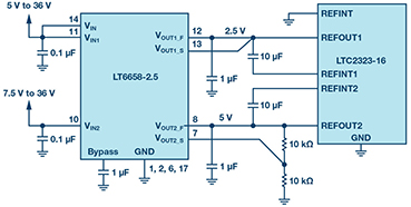 Figure 12. The LT6658 driving the LTC2323-16 dual ADC with independent voltage references.
Precision signal processing and conditioning can involve multiple integrated circuits. Figure 13 is an example where the LT6658 functions as a supply voltage and reference voltage for an 18-bit converter. A capacitive SAR converter is constantly charging and discharging an array of internal capacitors. The dynamic reference current of a SAR converter can wreak havoc on a voltage reference. The LT6658 can maintain stability by providing a precise voltage, while the second output can supply precision power. Moreover, the LT6658 has the current driving ability to supply voltage to multiple reference inputs. Another way to put this is the LT6658 has a large reference fan out ability.
Figure 12. The LT6658 driving the LTC2323-16 dual ADC with independent voltage references.
Precision signal processing and conditioning can involve multiple integrated circuits. Figure 13 is an example where the LT6658 functions as a supply voltage and reference voltage for an 18-bit converter. A capacitive SAR converter is constantly charging and discharging an array of internal capacitors. The dynamic reference current of a SAR converter can wreak havoc on a voltage reference. The LT6658 can maintain stability by providing a precise voltage, while the second output can supply precision power. Moreover, the LT6658 has the current driving ability to supply voltage to multiple reference inputs. Another way to put this is the LT6658 has a large reference fan out ability.
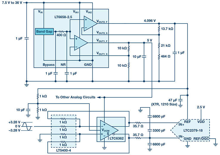 Figure 13. An 18-bit data acquisition application.
The buffers in the preceding applications provided a reference voltage to precision circuits. A valid concern is whether activity on the output of one buffer will affect the output of the other buffer. Supply rejection is >100 dB at dc continuing beyond 1 kHz when there is a 10 μF capacitor on the NR pin. This is when the VIN1 and VIN2 pins are connected together. See the LT6658 data sheet for details on ac PSRR. The channel-to-channel isolation supply to output is >130 dB at dc to 100 Hz.
Multichannel Output Supply with Tracking
Figure 13. An 18-bit data acquisition application.
The buffers in the preceding applications provided a reference voltage to precision circuits. A valid concern is whether activity on the output of one buffer will affect the output of the other buffer. Supply rejection is >100 dB at dc continuing beyond 1 kHz when there is a 10 μF capacitor on the NR pin. This is when the VIN1 and VIN2 pins are connected together. See the LT6658 data sheet for details on ac PSRR. The channel-to-channel isolation supply to output is >130 dB at dc to 100 Hz.
Multichannel Output Supply with Tracking
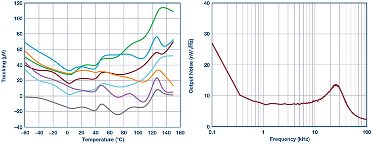 Figure 15a. Tracking. / Figure 15b. Output voltage noise density.
High Current, Low Temperature Coefficient Circuit Figure 16 illustrates how an LTC6655-2.5 low noise reference can overdrive the NR pin of the LT6658. The result is a dual output, low temperature coefficient (TC), high current reference. A variation of this circuit includes adding gain to one of the channels and driving the LTC6655’s VIN pin. The LTC6655-2.5 requires 500 mV headroom, necessitating a minimum 3 V output from one of the LT6658’s buffers. Figure 16. A low drift, high current application.
Power Applications
The buffer outputs can be combined to provide a single 200 mA output. The resistors allow the outputs to be connected together without wreaking havoc. The load regulation of the circuit in Figure 17 is limited by the value of the resistors and is 3 ppm/mA. This is in addition to the typical load regulation of the part at 0.25 μV/mA. The resistors can also be scaled to reduce the load regulation. And, since the resistance values are so low, power dissipation is not an issue.
The resistors can be constructed from a printed circuit board trace. One or two ounce copper can be used, or a combination of 0.01 Ω resistors can be arranged. This circuit will also sink current with the same ratios it sources current.
Figure 16. A low drift, high current application.
Power Applications
The buffer outputs can be combined to provide a single 200 mA output. The resistors allow the outputs to be connected together without wreaking havoc. The load regulation of the circuit in Figure 17 is limited by the value of the resistors and is 3 ppm/mA. This is in addition to the typical load regulation of the part at 0.25 μV/mA. The resistors can also be scaled to reduce the load regulation. And, since the resistance values are so low, power dissipation is not an issue.
The resistors can be constructed from a printed circuit board trace. One or two ounce copper can be used, or a combination of 0.01 Ω resistors can be arranged. This circuit will also sink current with the same ratios it sources current.
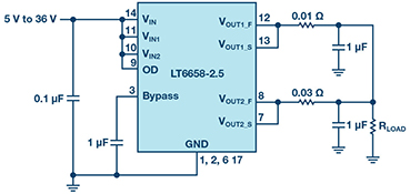 Figure 17. Parallel outputs for 200 mA output.
The two outputs will try to compensate each other requiring some resistance between them. There can be up to ±70 μV difference between the two outputs. Using the shown values of 0.01 Ω and 0.03 Ω, there are up to a few milliamps of current flowing between the output buffers. As the resistor values increase this shared current decreases. However, large isolation resistors mean a larger load regulation error as shown in Table 1.
Figure 17. Parallel outputs for 200 mA output.
The two outputs will try to compensate each other requiring some resistance between them. There can be up to ±70 μV difference between the two outputs. Using the shown values of 0.01 Ω and 0.03 Ω, there are up to a few milliamps of current flowing between the output buffers. As the resistor values increase this shared current decreases. However, large isolation resistors mean a larger load regulation error as shown in Table 1.
Table 1. Load Regulation as a Function of Output Resistors.
For applications that require lots of precision current, the LT6658 can be combined with a few transistors and ballast resistors to create a precision low noise, 5 A fixed dc supply, as shown in Figure 18.
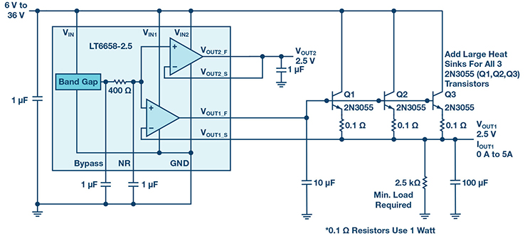 Figure 18. A precision, low noise fixed, 2.5 V, 5 A supply circuit.
A variable supply can be derived from Figure 18 with a few modifications, as shown in Figure 19. A blog article discusses this design, which can be found here.
Figure 18. A precision, low noise fixed, 2.5 V, 5 A supply circuit.
A variable supply can be derived from Figure 18 with a few modifications, as shown in Figure 19. A blog article discusses this design, which can be found here.
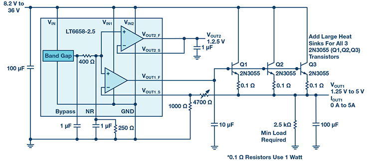 Figure 19. Precision, low noise variable, 1 V to 5 V, 5 A supply.
Supplying Power to a RF Circuit
The application in Figure 20 has the LT6658 providing power where one output is increased to 3 V and the other output is decreased to 1.4 V. This provides power to an I and Q signal amplifier/filter and modulator. The 3 V output supplies power to the filters and modulator, while the 1.4 V output sets the common mode. The LT6658’s OD pin is used to toggle the circuit between transmit and standby.
Figure 19. Precision, low noise variable, 1 V to 5 V, 5 A supply.
Supplying Power to a RF Circuit
The application in Figure 20 has the LT6658 providing power where one output is increased to 3 V and the other output is decreased to 1.4 V. This provides power to an I and Q signal amplifier/filter and modulator. The 3 V output supplies power to the filters and modulator, while the 1.4 V output sets the common mode. The LT6658’s OD pin is used to toggle the circuit between transmit and standby.
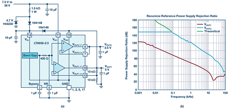 Figure 21. a) Extreme supply rejection circuit, b) AC power supply rejection ratio of the recursive reference.
A 24-Bit, High Resolution ADC Application
The AD7768-1 is a precision, 24-bit Σ-Δ converter designed for wide bandwidth, high density instrumentation, energy, and healthcare equipment. The AD7768-1 is a demanding converter that requires a low noise, precise, and solid voltage reference to drive its reference input pin. For this application, one output of the LT6658 provides 5 V to the analog supply pins AVDD1 and AVDD2. The other output provides 4.096 V to the reference input.
Figure 21. a) Extreme supply rejection circuit, b) AC power supply rejection ratio of the recursive reference.
A 24-Bit, High Resolution ADC Application
The AD7768-1 is a precision, 24-bit Σ-Δ converter designed for wide bandwidth, high density instrumentation, energy, and healthcare equipment. The AD7768-1 is a demanding converter that requires a low noise, precise, and solid voltage reference to drive its reference input pin. For this application, one output of the LT6658 provides 5 V to the analog supply pins AVDD1 and AVDD2. The other output provides 4.096 V to the reference input.
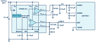 Figure 22. A 24-bit, simultaneously sampling Σ-Δ converter powered by the LT6658.
The resulting FFT with a 1 kHz input tone and the fastest available sampling rate is shown below in Figure 23. To put this in perspective, the 4.096 V reference is divided down to an LSB size of 488 nV. Any noise, ripple, or feedthrough becomes readily apparent in the measurement results.
Figure 22. A 24-bit, simultaneously sampling Σ-Δ converter powered by the LT6658.
The resulting FFT with a 1 kHz input tone and the fastest available sampling rate is shown below in Figure 23. To put this in perspective, the 4.096 V reference is divided down to an LSB size of 488 nV. Any noise, ripple, or feedthrough becomes readily apparent in the measurement results.
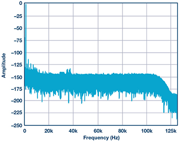 Figure 23. FFT of the AD7768-1 and LT6658 application.
Conclusion
The versatility and flexibility of the LT6658 is considered with a few applications. While the applications shown here use the 2.5 V variant, there are five other voltage options available, namely 1.2 V, 1.8 V, 3 V, 3.3 V, and 5 V. All six options share the same exacting specifications and rigorous testing Analog Devices is known for.
The LT6658 was conceived to satisfy customers who want more supply current from a voltage reference. Having two outputs seemed sensible and the aforementioned architecture emerged. As demonstrated in the preceding pages, this architecture can be exploited for various applications. Undoubtedly our customers will find many other innovative ways to apply the LT6658.
For more information on the capabilities of the LT6658 visit our website and look up the Analog Dialogue article The Refulator: The Capabilities of a 200 mA Precision Voltage Reference.
Acknowledgements
The circuits in the article were contributed, built, and tested from a wide source of talented people here at ADI. I would like to thank Philip Karantzalis, Noe Quintero, Niall McGinley, Robert Keily, and Tom Westenberg. I’d also like to thank Aaron Schultz and Catherine Chang for their helpful feedback on the article. And thanks to Brendan Whelan for his comments and support.
Figure 23. FFT of the AD7768-1 and LT6658 application.
Conclusion
The versatility and flexibility of the LT6658 is considered with a few applications. While the applications shown here use the 2.5 V variant, there are five other voltage options available, namely 1.2 V, 1.8 V, 3 V, 3.3 V, and 5 V. All six options share the same exacting specifications and rigorous testing Analog Devices is known for.
The LT6658 was conceived to satisfy customers who want more supply current from a voltage reference. Having two outputs seemed sensible and the aforementioned architecture emerged. As demonstrated in the preceding pages, this architecture can be exploited for various applications. Undoubtedly our customers will find many other innovative ways to apply the LT6658.
For more information on the capabilities of the LT6658 visit our website and look up the Analog Dialogue article The Refulator: The Capabilities of a 200 mA Precision Voltage Reference.
Acknowledgements
The circuits in the article were contributed, built, and tested from a wide source of talented people here at ADI. I would like to thank Philip Karantzalis, Noe Quintero, Niall McGinley, Robert Keily, and Tom Westenberg. I’d also like to thank Aaron Schultz and Catherine Chang for their helpful feedback on the article. And thanks to Brendan Whelan for his comments and support.
Mike Anderson [michael.anderson@analog.com] is a senior IC design engineer with © Analog Devices where he works on signal conditioning products such as precision references and amplifiers. He previously worked as a senior member of technical staff and section lead at Maxim Integrated Products, designing ADCs and mixed-signal circuits. Prior to 1997, Mike worked at Symbios Logic as a principle IC design engineer, designing high speed fiber channel circuits. He received a B.S.E.E. and an M.S.E.E. from Purdue University. Mike holds 16 patents and occasionally publishes articles.
- Source current: 150 mA and 50 mA
- Sink current: 20 mA/buffer
- Drift: 10 ppm/°C
- Accuracy: 0.05%
- Load regulation: 0.25 μV/mA
- Output tracking: ±150 μV
- PSRR: >100 dB at 10 Hz
- 0.1 Hz to 10 Hz noise: 1.5 ppm p-p
- Maximum supply: 36 V
- Noise reduction pin
- Output disable pin
- Current protection
- Thermal protection
- Small footprint
- Temperature range: –40°C to +125°C
Figure 1. The LT6658 typical application.
The output buffers are trimmed to minimize drift resulting in excellent tracking over operating and load conditions. The complete data sheet with specifications can be found here.
Simple Output Configurations and Applications
Since the inverting inputs are available they can be arranged for nonunity gain, as shown in Figure 2. A LT5400-4 has 0.01% matching maintaining the precision of the LT6658. This example provides a precise 5 V and 2.5 V rail and can be used as a ±2.5 V regulator application with a split supply ground provided by the 2.5 V output. Nonunity gain can be applied to both outputs to generate any output voltage between 1 V and 6 V.
Figure 2. Simple, nonunity gain circuit creating a ±2.5 V split supply with ground.
A lower output voltage can be generated from a higher output voltage using the inverting input. Figure 3 demonstrates how a 3.3 V output can be used to generate a 1.8 V output. Since the noninverting inputs are tied to 2.5 V, it’s simple to create a lower output voltage. The expression for VOUT2_F is ___ where RF1 and RF2 are the buffer feedback resistors and RIN1 and RIN2 are the buffer input resistors.
Figure 3. An application with gain and inversion.
The only parameter that is compromised in this application is accuracy, which is dependent on the ratios of RF/RIN. In addition, this application illustrates how the BYPASS output can be used as a ±10 mA source and sink output. Note that any change on the BYPASS pin will directly affect the VOUT1 and VOUT2 outputs.
The output voltages can be trimmed to values between 2.5 V and 6 V, as shown in Figure 4. The trims can be accomplished with mechanical trim or digital trim pots. Digital trim is especially helpful to correct for ADC and DAC errors. The trim pots can be ganged to produce the same output voltage or the outputs voltages can be independently controlled.
Figure 4. Adjustable gain.
Having two output buffers provides flexibility where one output can provide a necessary voltage, and the other output can provide a precision current source, as shown in Figure 5.
Note that the output VOUT2_F pin will be one VBE higher than the sense line. The supply voltage should be adjusted to accommodate the higher output voltage on VOUT2_F. Since each output has an independent supply input, they can be driven separately to improve channel-to-channel isolation or to accommodate different output voltages without consuming excessive power.
Figure 5. A precision voltage source and a precision current source application.
Typically, when one mentions a voltage reference and oscillation in the same sentence, they are referring to undesirable behavior. However, to highlight the unique architecture of the LT6658, the multivibrator circuit in Figure 6a is introduced, along with the resulting waveforms in Figure 6b. Here a 2.2 μF capacitor and 1 kΩ resistor set the time constant. The 400 Ω external positive feedback resistor and 400 Ω internal resistor set the hysteresis and affect the output frequency, which is roughly
f = 1/2.2 RC. The value of the internal resistor is 400 Ω ±15%, which will affect the output frequency.
Figure 6a. Multivibrator application. / Figure 6b. Multivibrator output.
This circuit example shows the output voltage swing is slightly less than 4 V where the output low voltage goes down to 0.9 V and the output high voltage reaches to VIN – 2.5 V. VIN in this example is 6 V and the output is not fully loaded. As VIN increases past 8.5 V, the output will clamp around 6 V and the output duty cycle will reduce to about 40%.
Since current is flowing through the 400 Ω internal resistor, the voltage at the NR pin varies, causing VOUT1 to also oscillate synchronously with VOUT2.
Another dynamic circuit that is usually not associated with a voltage reference is the audio amplifier. The dual class A/B outputs can be arranged to drive 8 Ω and 16 Ω speakers, as shown in Figure 7. A single-ended source drives the inverting input of VOUT1, which drives the inverting input of VOUT2. The band gap sets a precision common mode, while the outputs act as a differential driver. To improve slew rate, use the minimum output capacitance on the LT6658.
Figure 7. An audio application circuit.
With the addition of complementary discrete BJT output devices, the circuit in Figure 8 can supply more power. The circuit shows only one amplifier circuit, though two speakers can be driven by the two outputs to create stereo. While there are better audio amplifier choices, these applications demonstrate the flexibility of the LT6658 architecture.
Figure 8. An audio application circuit using discrete BJTs.
Strain Gage Applications
The LT6658 can act as a regulator and a reference, as shown in the following strain gage application (Figure 9). The LT6658 provides the reference voltage and supply voltage to four LTC2440, and the 2.5 V rail biases the four strain gages. Each strain gage draws 7.5 mA totaling 30 mA, which is well within VOUT2’s 50 mA output specification and provides the ADC reference input. VOUT1 supplies 8 mA to each LTC2440 for a total of 32 mA.
Figure 9. The LT6658 as a reference and regulator for a strain gage application.
Figure 10 shows a bridge circuit application with three load cells. The LT6658 provides a precise and stable operation even though the total load resistance is only 82 Ω requiring 60 mA. The high gain buffer will maintain a precise voltage capable of driving the load cells. The second output can drive another strain gage or supply power to the ADC converter downstream.
Figure 10. A bridge circuit application.
Data Acquisition Applications
For precision applications that use a DAC where the reference current is code dependent, it is important to pay special attention to board layout and parasitic resistance. To maintain an INL < 0.1 LSB with the LTC2641, load regulation needs to be <19 ppm/mA. Further, reference output impedance and PCB resistance needs to be <48 mW. The LT6658 has a dc output resistance of about 0.2 mW, leaving a 47.8 mW error budget for PCB resistance.
Figure 11 shows an application with two LTC2641 precision, 16-bit DACs. Since the reference current of the LTC2641 is code dependent, the two DAC reference inputs require a separate reference. The exception tracking of LT6658 output buffers translates into exceptional tracking of the DACs.
If only one DAC is required, the second output of the LT6658 can supply the input voltage to the DAC and other precision analog circuitry.
Figure 11. The LT6658 driving two code dependent DAC reference inputs.
The LTC2323-16 is a dual, 16-bit ADC with separate reference inputs. This allows for a different reference voltage for each ADC. Figure 12 shows one arrangement where 2.5 V and 5 V reference voltages drive the separate reference inputs. Again, the LT6658 output buffers track well maintaining conversion results that also track.
Figure 12. The LT6658 driving the LTC2323-16 dual ADC with independent voltage references.
Precision signal processing and conditioning can involve multiple integrated circuits. Figure 13 is an example where the LT6658 functions as a supply voltage and reference voltage for an 18-bit converter. A capacitive SAR converter is constantly charging and discharging an array of internal capacitors. The dynamic reference current of a SAR converter can wreak havoc on a voltage reference. The LT6658 can maintain stability by providing a precise voltage, while the second output can supply precision power. Moreover, the LT6658 has the current driving ability to supply voltage to multiple reference inputs. Another way to put this is the LT6658 has a large reference fan out ability.
Figure 13. An 18-bit data acquisition application.
The buffers in the preceding applications provided a reference voltage to precision circuits. A valid concern is whether activity on the output of one buffer will affect the output of the other buffer. Supply rejection is >100 dB at dc continuing beyond 1 kHz when there is a 10 μF capacitor on the NR pin. This is when the VIN1 and VIN2 pins are connected together. See the LT6658 data sheet for details on ac PSRR. The channel-to-channel isolation supply to output is >130 dB at dc to 100 Hz.
Multichannel Output Supply with Tracking
The NR pins of several LT6658s can be tied together creating a multichannel precision supply with tracking. In the example shown in Figure 14, four LT6658s have their NR pins tied together. The resulting supply has eight tracking outputs. That is, since all the NR pins are tied together, the output buffers in each of four LT6658s will track over temperature. Figure 15a shows how the precision trimmed outputs track over a wide temperature range. The seven traces in this plot are referred to the first VOUT1. This demonstrates the low offset voltage and the low temperature drift of the output buffers. By tying the NR pins together, the input voltage to the buffers are the same, and the CNR capacitors will combine to a larger value reducing the noise bandwidth coming of the band gap circuits. The resulting noise density spectrum at the output buffer is shown in Figure 15b, where the noise is dominated by the output buffer and the bandgap noise rolls at less than 10 Hz. This example shows all the channels configured as unity gain. The output voltages can be configured for a variety of output voltage values. While these devices share the NR pin and supply voltage, they retain excellent PSRR, load isolation, and load regulation.Figure 14. Paralleled NR pins for multichannel supplies with output tracking. This image has zoom function.
Figure 15a. Tracking. / Figure 15b. Output voltage noise density.
High Current, Low Temperature Coefficient Circuit Figure 16 illustrates how an LTC6655-2.5 low noise reference can overdrive the NR pin of the LT6658. The result is a dual output, low temperature coefficient (TC), high current reference. A variation of this circuit includes adding gain to one of the channels and driving the LTC6655’s VIN pin. The LTC6655-2.5 requires 500 mV headroom, necessitating a minimum 3 V output from one of the LT6658’s buffers.
Figure 16. A low drift, high current application.
Power Applications
The buffer outputs can be combined to provide a single 200 mA output. The resistors allow the outputs to be connected together without wreaking havoc. The load regulation of the circuit in Figure 17 is limited by the value of the resistors and is 3 ppm/mA. This is in addition to the typical load regulation of the part at 0.25 μV/mA. The resistors can also be scaled to reduce the load regulation. And, since the resistance values are so low, power dissipation is not an issue.
The resistors can be constructed from a printed circuit board trace. One or two ounce copper can be used, or a combination of 0.01 Ω resistors can be arranged. This circuit will also sink current with the same ratios it sources current.
Figure 17. Parallel outputs for 200 mA output.
The two outputs will try to compensate each other requiring some resistance between them. There can be up to ±70 μV difference between the two outputs. Using the shown values of 0.01 Ω and 0.03 Ω, there are up to a few milliamps of current flowing between the output buffers. As the resistor values increase this shared current decreases. However, large isolation resistors mean a larger load regulation error as shown in Table 1.
| R1 (Ω) | R2 (Ω) | Load Regulation (ppm/mA) |
| 0.01 | 0.03 | 3 |
| 0.02 | 0.06 | 6 |
| 0.03 | 0.09 | 9 |
| 0.04 | 0.12 | 12 |
| 0.05 | 0.15 | 15 |
Figure 18. A precision, low noise fixed, 2.5 V, 5 A supply circuit.
A variable supply can be derived from Figure 18 with a few modifications, as shown in Figure 19. A blog article discusses this design, which can be found here.
Figure 19. Precision, low noise variable, 1 V to 5 V, 5 A supply.
Supplying Power to a RF Circuit
The application in Figure 20 has the LT6658 providing power where one output is increased to 3 V and the other output is decreased to 1.4 V. This provides power to an I and Q signal amplifier/filter and modulator. The 3 V output supplies power to the filters and modulator, while the 1.4 V output sets the common mode. The LT6658’s OD pin is used to toggle the circuit between transmit and standby.
Recursive Reference While the LT6658 has exceptional power supply rejection, Figure 21 takes power supply rejection to the next level. The recursive reference shown in Figure 21 creates an output on VOUT2 that is extremely isolated from the supply voltage. VIN1 and VIN are driven by the external supply and creates a 5 V supply on VOUT1. Once active, VOUT1 then takes over powering VIN and subsequently, VIN2, isolating those supply inputs from the external supply. As the plot in Figure 21b shows, the measurable low frequency supply rejection is over 140 dB at the limit of our test setup. A theoretical trace is included that indicates the more likely supply rejection.Figure 20. A low power, low noise I and Q signal amplifier/filter and modulator. Image with zoom function.
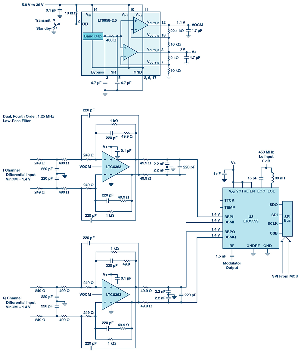 Figure 21. a) Extreme supply rejection circuit, b) AC power supply rejection ratio of the recursive reference.
A 24-Bit, High Resolution ADC Application
The AD7768-1 is a precision, 24-bit Σ-Δ converter designed for wide bandwidth, high density instrumentation, energy, and healthcare equipment. The AD7768-1 is a demanding converter that requires a low noise, precise, and solid voltage reference to drive its reference input pin. For this application, one output of the LT6658 provides 5 V to the analog supply pins AVDD1 and AVDD2. The other output provides 4.096 V to the reference input.
Figure 22. A 24-bit, simultaneously sampling Σ-Δ converter powered by the LT6658.
The resulting FFT with a 1 kHz input tone and the fastest available sampling rate is shown below in Figure 23. To put this in perspective, the 4.096 V reference is divided down to an LSB size of 488 nV. Any noise, ripple, or feedthrough becomes readily apparent in the measurement results.
Figure 23. FFT of the AD7768-1 and LT6658 application.
Conclusion
The versatility and flexibility of the LT6658 is considered with a few applications. While the applications shown here use the 2.5 V variant, there are five other voltage options available, namely 1.2 V, 1.8 V, 3 V, 3.3 V, and 5 V. All six options share the same exacting specifications and rigorous testing Analog Devices is known for.
The LT6658 was conceived to satisfy customers who want more supply current from a voltage reference. Having two outputs seemed sensible and the aforementioned architecture emerged. As demonstrated in the preceding pages, this architecture can be exploited for various applications. Undoubtedly our customers will find many other innovative ways to apply the LT6658.
For more information on the capabilities of the LT6658 visit our website and look up the Analog Dialogue article The Refulator: The Capabilities of a 200 mA Precision Voltage Reference.
Acknowledgements
The circuits in the article were contributed, built, and tested from a wide source of talented people here at ADI. I would like to thank Philip Karantzalis, Noe Quintero, Niall McGinley, Robert Keily, and Tom Westenberg. I’d also like to thank Aaron Schultz and Catherine Chang for their helpful feedback on the article. And thanks to Brendan Whelan for his comments and support.
Figure 21. a) Extreme supply rejection circuit, b) AC power supply rejection ratio of the recursive reference.
A 24-Bit, High Resolution ADC Application
The AD7768-1 is a precision, 24-bit Σ-Δ converter designed for wide bandwidth, high density instrumentation, energy, and healthcare equipment. The AD7768-1 is a demanding converter that requires a low noise, precise, and solid voltage reference to drive its reference input pin. For this application, one output of the LT6658 provides 5 V to the analog supply pins AVDD1 and AVDD2. The other output provides 4.096 V to the reference input.
Figure 22. A 24-bit, simultaneously sampling Σ-Δ converter powered by the LT6658.
The resulting FFT with a 1 kHz input tone and the fastest available sampling rate is shown below in Figure 23. To put this in perspective, the 4.096 V reference is divided down to an LSB size of 488 nV. Any noise, ripple, or feedthrough becomes readily apparent in the measurement results.
Figure 23. FFT of the AD7768-1 and LT6658 application.
Conclusion
The versatility and flexibility of the LT6658 is considered with a few applications. While the applications shown here use the 2.5 V variant, there are five other voltage options available, namely 1.2 V, 1.8 V, 3 V, 3.3 V, and 5 V. All six options share the same exacting specifications and rigorous testing Analog Devices is known for.
The LT6658 was conceived to satisfy customers who want more supply current from a voltage reference. Having two outputs seemed sensible and the aforementioned architecture emerged. As demonstrated in the preceding pages, this architecture can be exploited for various applications. Undoubtedly our customers will find many other innovative ways to apply the LT6658.
For more information on the capabilities of the LT6658 visit our website and look up the Analog Dialogue article The Refulator: The Capabilities of a 200 mA Precision Voltage Reference.
Acknowledgements
The circuits in the article were contributed, built, and tested from a wide source of talented people here at ADI. I would like to thank Philip Karantzalis, Noe Quintero, Niall McGinley, Robert Keily, and Tom Westenberg. I’d also like to thank Aaron Schultz and Catherine Chang for their helpful feedback on the article. And thanks to Brendan Whelan for his comments and support.Mike Anderson [michael.anderson@analog.com] is a senior IC design engineer with © Analog Devices where he works on signal conditioning products such as precision references and amplifiers. He previously worked as a senior member of technical staff and section lead at Maxim Integrated Products, designing ADCs and mixed-signal circuits. Prior to 1997, Mike worked at Symbios Logic as a principle IC design engineer, designing high speed fiber channel circuits. He received a B.S.E.E. and an M.S.E.E. from Purdue University. Mike holds 16 patents and occasionally publishes articles.