


© AT&S
Products |
Interconnection technologies for next-generation 5G mobile communications
Innovative solution concepts based on new materials, hybrid printed circuit board (PCB) structures with various technologies and embedded circuits.
This is a product release announcement by AT&S Austria Technologie & Systemtechnik Aktiengesellschaft. The issuer is solely responsible for its content.
Significantly higher data rates and volumes together with high power densities are resulting in rising requirements for interconnection technologies, too. The new 5G mobile communications generation is undoubtedly an overarching and defining trend here, with applications ranging from infrastructure (base stations) to terminal devices (mobile phones), as well as real-time automation scenarios. AT&S is supporting the current roll-out of the 5G mobile communications generation with high frequency (HF) optimized interconnect solutions and will continue to offer corresponding solutions as the new standard develops.
The launch of the 5G mobile communications generation has far-reaching consequences on the product and system level in terms of miniaturization, functional integration, electromagnetic compatibility (EMC), signal integrity, modularity, safety, security, etc. AT&S therefore analyzed customer requirements and implications for the PCB, substrate and packaging, then initiated and implemented appropriate developments. Innovative solution concepts respond to the challenges of 5G, e.g. using new materials, combining different technologies for hybrid PCB structures, and embedding passive and active circuit components. AT&S invested not only in processes and materials, but also in essential HF measurement equipment to investigate transmission losses, phase shifts and signal delays at up to 100 GHz, for example.
The roll-out of the new 5G mobile communications generation, with frequency bands up to 6 GHz, is already underway. The next step will be to implement 5G millimeter waves with frequencies of 28 GHz or even higher. In principle, for an interconnection technology manufacturer like AT&S, this means reducing signal losses and interference, e.g. by optimizing the dielectric layer in respect of the material (dielectric constant) or thickness, the material transitions (interfaces), or also the copper roughness.
With copper, the major challenge is that while smoother copper offers advantages for HF applications, somewhat greater roughness improves the adhesion of the PCB traces on the basic material. For this reason, AT&S conducted an extensive study of commercially available copper foils for HF applications. The geometry (profile) of the tracks also affects signal delays at higher frequencies and has to be optimized. In addition, AT&S investigated the effects between different metals (copper, gold, nickel) on the skin effect in the GHz range and is developing new surface materials accordingly to get optimized results.
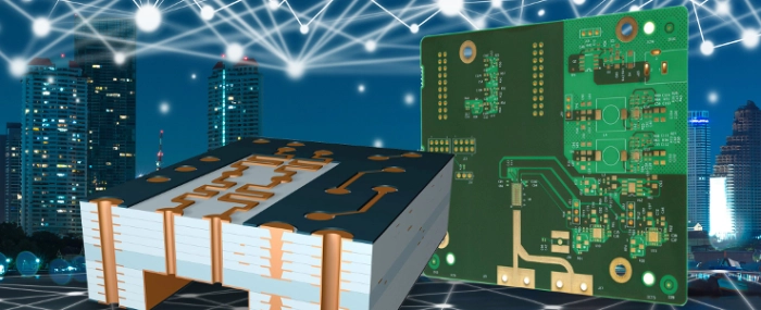
For 5G applications, a hybrid PCB structure combining high-speed layers (HF-optimized) and standard layers represents a performance and cost-optimized solution. AT&S has created a 12-layer hybrid board (HF and FR4 in 2.5D technology) for wireless systems with fully integrated HF antenna. The layers are connected by micro-vias (filled and stacked). Another exemplary HF-optimized solution is a 6-layer board that combines HF layers having a very low dielectric constant with embedded components (application-specific integrated circuits (ASICs) under the antenna structure). The connection between ASICs and antenna is formed by laser-vias.
.png)