


© janaka dharmasena / dreamstime.com
Application Notes |
What’s in your portable product?
We are all familiar with batteries these days; they are virtually ubiquitous in a myriad of products and applications.
Commonplace examples include your cell phone and notebook computer; however, they are also commonly found in flashlights, cordless tools, MP3 players, portable video gaming devices, hand-held multi-meters, as well as, scientific instruments and a rapidly expanding plethora of healthcare devices.
Accordingly, it will come as no surprise to learn that the global market for portable battery-powered products was valued at an estimated $480B in 2011 and is expected to reach more than $611B in 2016. [Source: BCC Research]. Furthermore, this market is expected to continue its growth expansion through to 2020.
This market can be roughly segmented as follows:
 Figure 1. LTC3119 Schematic Showing a High Level of Integration & Performance
Many portable systems require being powered from multiple input sources including single or multi-call battery configurations, wall adapters and supercapacitor stacks. Another device within the same family as the LTC3119 is the LTC3118, a dual input, monolithic buck-boost with integrated lossless PowerPath™ which is capable of delivering up to 2A of continuous output current. The LTC3118 integrates the intelligence to automatically transition to the proper input source to seamlessly maintain a regulated output. Each input can operate from 2.2Vto 18V, while the output can be programmed between 2V and 18V making the part suitable for a wide variety of applications. The LTC3118 employs a low noise, current mode buck-boost topology architecture with a fixed1.2MHz switching frequency. Its unique design provides a continuous, jitter-free transition between buck and boost modes, making it ideal for RF and other noise-sensitive applications. The combination of tiny externals and a 4mm x 5mm QFN or TSSOP-28E package provides a compact solution footprint. See Figure 2 for its simplified schematic.
The LTC3118 includes four internal low RDS(ON) N-channel MOSFETs to deliver efficiencies of up to 94% from either input. User-selectable Burst Mode operation lowers input quiescent current to only 50μA, improving light load efficiency and extending battery run time. For noise-sensitive applications, Burst Mode operation can be disabled resulting in fixed frequency, low-noise operation independent of load current. Other features include soft-start, overvoltage protection, short-circuit protection, thermal shutdown and output disconnect.
Figure 1. LTC3119 Schematic Showing a High Level of Integration & Performance
Many portable systems require being powered from multiple input sources including single or multi-call battery configurations, wall adapters and supercapacitor stacks. Another device within the same family as the LTC3119 is the LTC3118, a dual input, monolithic buck-boost with integrated lossless PowerPath™ which is capable of delivering up to 2A of continuous output current. The LTC3118 integrates the intelligence to automatically transition to the proper input source to seamlessly maintain a regulated output. Each input can operate from 2.2Vto 18V, while the output can be programmed between 2V and 18V making the part suitable for a wide variety of applications. The LTC3118 employs a low noise, current mode buck-boost topology architecture with a fixed1.2MHz switching frequency. Its unique design provides a continuous, jitter-free transition between buck and boost modes, making it ideal for RF and other noise-sensitive applications. The combination of tiny externals and a 4mm x 5mm QFN or TSSOP-28E package provides a compact solution footprint. See Figure 2 for its simplified schematic.
The LTC3118 includes four internal low RDS(ON) N-channel MOSFETs to deliver efficiencies of up to 94% from either input. User-selectable Burst Mode operation lowers input quiescent current to only 50μA, improving light load efficiency and extending battery run time. For noise-sensitive applications, Burst Mode operation can be disabled resulting in fixed frequency, low-noise operation independent of load current. Other features include soft-start, overvoltage protection, short-circuit protection, thermal shutdown and output disconnect.
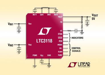 Figure 2. LTC3118 Schematic with PowerPath Section between Two Inputs
Conclusion
A large opportunity has presented itself for designing a wide range of battery powered portable products to meet the growing appetite for communications, medical and computer related products. System designers have faced some difficult challenges in selecting the right power conversion solution that meets the key design objectives, including spanning the input-to-output voltage constraints, power levels and ease of design, without compromising efficiency, run time and solution size.
Designing a solution that meets the system goals without a performance impact can be a daunting task. Fortunately, there are a growing number of buck-boost converter solutions from Linear Technology, which simplify the design, offer best-in-class features and have the ability to maximize run times in-between battery recharging cycles due to their high efficiency operation across a wide range of loads.
Figure 2. LTC3118 Schematic with PowerPath Section between Two Inputs
Conclusion
A large opportunity has presented itself for designing a wide range of battery powered portable products to meet the growing appetite for communications, medical and computer related products. System designers have faced some difficult challenges in selecting the right power conversion solution that meets the key design objectives, including spanning the input-to-output voltage constraints, power levels and ease of design, without compromising efficiency, run time and solution size.
Designing a solution that meets the system goals without a performance impact can be a daunting task. Fortunately, there are a growing number of buck-boost converter solutions from Linear Technology, which simplify the design, offer best-in-class features and have the ability to maximize run times in-between battery recharging cycles due to their high efficiency operation across a wide range of loads.
Author: Tony Armstrong, Director or Product Marketing, Power Products, © Linear Technology (now part of Analog Devices)
- ~29% for communication products
- ~29% for the computer related products
- ~19% for medical product
- ~23% for cameras, toys, entertainment, timepieces, lighting, navigation and military products
Figure 1. LTC3119 Schematic Showing a High Level of Integration & Performance
Many portable systems require being powered from multiple input sources including single or multi-call battery configurations, wall adapters and supercapacitor stacks. Another device within the same family as the LTC3119 is the LTC3118, a dual input, monolithic buck-boost with integrated lossless PowerPath™ which is capable of delivering up to 2A of continuous output current. The LTC3118 integrates the intelligence to automatically transition to the proper input source to seamlessly maintain a regulated output. Each input can operate from 2.2Vto 18V, while the output can be programmed between 2V and 18V making the part suitable for a wide variety of applications. The LTC3118 employs a low noise, current mode buck-boost topology architecture with a fixed1.2MHz switching frequency. Its unique design provides a continuous, jitter-free transition between buck and boost modes, making it ideal for RF and other noise-sensitive applications. The combination of tiny externals and a 4mm x 5mm QFN or TSSOP-28E package provides a compact solution footprint. See Figure 2 for its simplified schematic.
The LTC3118 includes four internal low RDS(ON) N-channel MOSFETs to deliver efficiencies of up to 94% from either input. User-selectable Burst Mode operation lowers input quiescent current to only 50μA, improving light load efficiency and extending battery run time. For noise-sensitive applications, Burst Mode operation can be disabled resulting in fixed frequency, low-noise operation independent of load current. Other features include soft-start, overvoltage protection, short-circuit protection, thermal shutdown and output disconnect.
Figure 2. LTC3118 Schematic with PowerPath Section between Two Inputs
Conclusion
A large opportunity has presented itself for designing a wide range of battery powered portable products to meet the growing appetite for communications, medical and computer related products. System designers have faced some difficult challenges in selecting the right power conversion solution that meets the key design objectives, including spanning the input-to-output voltage constraints, power levels and ease of design, without compromising efficiency, run time and solution size.
Designing a solution that meets the system goals without a performance impact can be a daunting task. Fortunately, there are a growing number of buck-boost converter solutions from Linear Technology, which simplify the design, offer best-in-class features and have the ability to maximize run times in-between battery recharging cycles due to their high efficiency operation across a wide range of loads.Author: Tony Armstrong, Director or Product Marketing, Power Products, © Linear Technology (now part of Analog Devices)
