

© panasonic
Business |
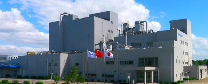
Panasonic starts production of molded underfill materials
Panasonic will launch the mass production of molded underfill semiconductor encapsulation materials in Shanghai, China in response to the increased production of semiconductor packages in the region.
Along with the increasing domestic demand and growing exports, Chinese electronics manufacturers are increasing production of smartphones and other portable electronic devices. As a result, outsourced semiconductor assembly, test contractors(OSATs) and other semiconductor manufacturers are boosting their production volumes. The higher performance and increased functionality of new smartphones is driving high-density semiconductor packaging technology development. As a result,, demand for MUF materials is growing. And in order to grab as much of this pie as possible, Panasonic will launch the production of MUF materials at PIDMSH in March 2018.
MUF materials are designed to encapsulate and protect the Flip chip semiconductor die and the electrical connections between the die and the semiconductor package circuit board. MUF materials encapsulate the entire semiconductor package without the need for a subsequent underfilling process.
In addition to the production site in China, Panasonic produces MUF materials in Yokkaichi-city, Mie Prefecture in Japan.
