


Application Notes |
Power management for FPGA, GPU and ASIC systems
There are only a few power management related design challenges on system boards controlled by FPGAs, GPUs, or ASICs, but these challenges can seriously delay release of a system due to repetitive debugging.
This is a product release announcement by Linear Technology Corporation. The issuer is solely responsible for its content.
However, many power and DC/DC regulation issues can be prevented if the very design or a similar design had been verified by the suppliers of power products and FPGA, GPU and ASIC manufacturers. The burden is often on the shoulders of system designers to analyze the problem, then find a solution. These engineers are already immersed in configuring the complex digital portions of the design. Tackling the analog and power portion of the design becomes a major challenge, since power is not the simple task that many designers expect.
Thoughtful Power Management is Challenging in the Beginning
Every design task is initially challenging, including power management for a complicated system with transceivers, memory modules, sensors, line connectors and mesh of PCB traces and layers of PCB planes. But haphazardly addressing power management with DC/DC regulators, capacitors, inductors, heat removal and heat sink, and layout of components can lead to later design problems. Hasty decisions by the system designer to choose inferior solutions will at some point will inhibit progress with debugging procedures.
Where to Begin Power Management
The start of any power management circuit can be done with confidence in a systematic and thoughtful way. In other words, it can be simplified if the analysis is accurate and addresses power management related design challenges before PCB assembly. Moreover, a power management guide is already tested and verified to meet the requirements of the FPGAs, ASICs, GPUs and microprocessors and the systems that use these and other digital components. Mapping power management with proven power management solutions will ensure that the project is initiated with high confidence. This is key to quickly turn a design from its prototyping stage to production: spend less time on debugging power.
Case in Point: Powering Arria 10 FPGA and Arria 10 SoC
FPGA development kits enable system developers to evaluate an FPGA without having to design a complete system. Figures 1 and 2 show Altera’s new 20nm Arria 10 FPGAs and Arria 10 SoCs (system-on-chip) development boards. These boards are tested and verified by Altera, exemplifying best design practices in layout, signal integrity and power management.
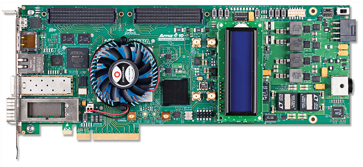 Figure 1: Arria 10 GX FPGA Development Kit board
Power Management for Core, System and I/O. The power management solution for high end FPGAs, including the Arria 10, should be carefully selected.
A well thought out power management design can reduce PCB size, weight and complexity, as well as lower power consumption and cooling costs. This is essential to achieve optimal system performance.
Figure 1: Arria 10 GX FPGA Development Kit board
Power Management for Core, System and I/O. The power management solution for high end FPGAs, including the Arria 10, should be carefully selected.
A well thought out power management design can reduce PCB size, weight and complexity, as well as lower power consumption and cooling costs. This is essential to achieve optimal system performance.
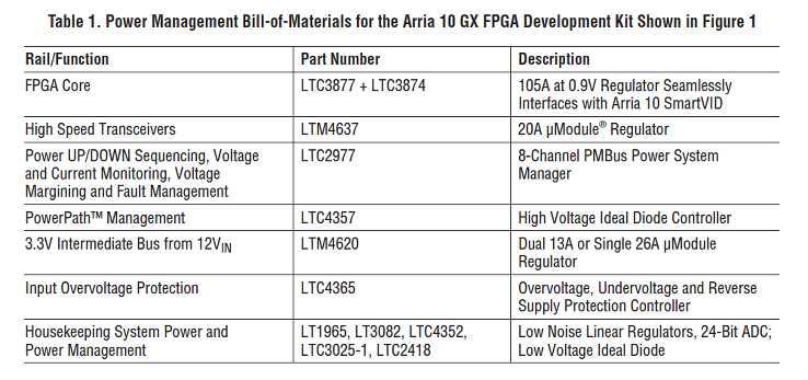 Table 1 summarizes the Arria 10 development kit’s power rails and functions shown in Figure 1. The table lists Linear Technology parts and descriptions for each function. Visit www.linear.com/altera , click on Arria and access technical details for the two boards presented here.
Customize the Power Tree with the LTpowerPlanner Design Tool
What if your power requirements differ from the designs exemplified in a development kit? In these cases, use the LTpowerPlanner® PC-based design tool to personalize and optimize a system’s power tree.
Start with the suggestions given in the development kit; then easily reorganize power blocks, alter power ratings, compute efficiency and power loss, simulate each power block, select DC/DC regulator part numbers and authenticate a customized solution.
LTpowerPlanner was used to generate the power trees (Figure 3) for the Arria 10 development kit’s FPGA and system requirements, and is available within the more encompassing LTpowerCAD® design tool, available for free download at www.linear.com/ltpowercad.
LTpowerCAD enables users to:
Table 1 summarizes the Arria 10 development kit’s power rails and functions shown in Figure 1. The table lists Linear Technology parts and descriptions for each function. Visit www.linear.com/altera , click on Arria and access technical details for the two boards presented here.
Customize the Power Tree with the LTpowerPlanner Design Tool
What if your power requirements differ from the designs exemplified in a development kit? In these cases, use the LTpowerPlanner® PC-based design tool to personalize and optimize a system’s power tree.
Start with the suggestions given in the development kit; then easily reorganize power blocks, alter power ratings, compute efficiency and power loss, simulate each power block, select DC/DC regulator part numbers and authenticate a customized solution.
LTpowerPlanner was used to generate the power trees (Figure 3) for the Arria 10 development kit’s FPGA and system requirements, and is available within the more encompassing LTpowerCAD® design tool, available for free download at www.linear.com/ltpowercad.
LTpowerCAD enables users to:
Figure 1: Arria 10 GX FPGA Development Kit board
Power Management for Core, System and I/O. The power management solution for high end FPGAs, including the Arria 10, should be carefully selected.
A well thought out power management design can reduce PCB size, weight and complexity, as well as lower power consumption and cooling costs. This is essential to achieve optimal system performance.
For example, the 0.95V at 105A, supplied by the 12V DC/DC regulator powering the core of the Arria 10 GX FPGA in Figure 1, has several features that complement the power saving schemes of the SoC: The DC/DC regulator’s integrated 6-bit parallel VID interface is used by the Arria 10’s SmartVID to control the DC/DC regulator and reduce FPGA power consumption during static and dynamic states. The DC/DC regulator’s very low value DCR current sensing improves efficiency by minimizing power loss in the inductor. Temperature compensation maintains the accuracy or the DCR value at higher inductor temperature.Figure 2: Arria 10 SoC Development Kit board -----
Figure 3: Power tree for Arria 10 GX FPGA board (Figure 1). Designed in LTpowerPlanner, an analytical and simple first step design tool for mapping power requirements.

 Table 1 summarizes the Arria 10 development kit’s power rails and functions shown in Figure 1. The table lists Linear Technology parts and descriptions for each function. Visit www.linear.com/altera , click on Arria and access technical details for the two boards presented here.
Customize the Power Tree with the LTpowerPlanner Design Tool
What if your power requirements differ from the designs exemplified in a development kit? In these cases, use the LTpowerPlanner® PC-based design tool to personalize and optimize a system’s power tree.
Start with the suggestions given in the development kit; then easily reorganize power blocks, alter power ratings, compute efficiency and power loss, simulate each power block, select DC/DC regulator part numbers and authenticate a customized solution.
LTpowerPlanner was used to generate the power trees (Figure 3) for the Arria 10 development kit’s FPGA and system requirements, and is available within the more encompassing LTpowerCAD® design tool, available for free download at www.linear.com/ltpowercad.
LTpowerCAD enables users to:
Table 1 summarizes the Arria 10 development kit’s power rails and functions shown in Figure 1. The table lists Linear Technology parts and descriptions for each function. Visit www.linear.com/altera , click on Arria and access technical details for the two boards presented here.
Customize the Power Tree with the LTpowerPlanner Design Tool
What if your power requirements differ from the designs exemplified in a development kit? In these cases, use the LTpowerPlanner® PC-based design tool to personalize and optimize a system’s power tree.
Start with the suggestions given in the development kit; then easily reorganize power blocks, alter power ratings, compute efficiency and power loss, simulate each power block, select DC/DC regulator part numbers and authenticate a customized solution.
LTpowerPlanner was used to generate the power trees (Figure 3) for the Arria 10 development kit’s FPGA and system requirements, and is available within the more encompassing LTpowerCAD® design tool, available for free download at www.linear.com/ltpowercad.
LTpowerCAD enables users to:
- Select specific Linear Technology DC/DC regulators to match a given power specification
- Select appropriate power components such as inductors, resistors and capacitors
- Optimize efficiency and power loss
- Optimize regulator loop stability, output impedance and load transient response
- Export the design to LTspice®