Ad
Ad
Ad
Ad
Ad
Ad
Ad
Ad
© janaka dharmasena dreamstime.com_technical
Application Notes |

Low-cost LED driver module 0.5 A / 33 VDC with >90% efficiency for general use

This article describes simple constant current driver module with fast PWM input that can be used for driving middle and high power LEDs.

The module uses Taiwan Semiconductor TSC19376 LED driver, operates from 8 to 33 VDC and the output current can be configured from 0.1 to 0.5 A in several steps. This article outlines component selection in order to implement this solution into a design.
Fig. 1. LED driver schematic ----- Fig. 2. Current and voltage waveform at switching node (GND oscilloscope connected to Vcc) ----- Fig. 3. LED Driver module connection diagram -----
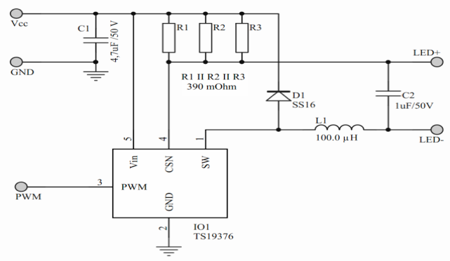
Specification:
  • Topology: Buck
  • Regulation: Hysteretic
  • Input voltage: 8-33 VDC
  • Output current: 100-500 mA
  • Switching frequency: 1 MHz max
  • Current ratio: 0.13 Ω / 1 A
  • Dimensions: 16 x 16 x 5.5 mm (0.63 x 0.63 x 0.22 in)
  • Weight: 1.6 g
  • Thermal shutdown
  • Over Current protection
  • Dimming: PWM up to 20 kHz
Short description LED driver module (Fig.1) is built on buck driver IC TS19376 in SOT89-5 package produced by Taiwan Semiconductor. This buck driver involves hysteretic regulation for relatively high efficiencies above 90% without need for compensation. Output current is set by the combination of parallel resistors R1-R3 (Fig.1) with a ratio of 0.13 Ω/1 A. Hysteretic regulation outlined in [1] can be shortly described: The internal switch of the TS19376 driver connects the input voltage to the load through inductor L1. Current through the inductor is linearly increased and monitored as voltage drop on R1 II R2 II R3). Once the current reaches 149.5 mV (130 mV + Vcsn_hys (15% = 19.5 mV)), the integrated switch turns off and current flowing through the inductor and D1 linearly decreases until it drops to 110.5 mV (130 mV – Vcsn_hys (15% = 19.5 mV)), when the switch turns again on and this process repeats for each cycle as shown in Fig.2. The switching frequency is given by output current (ILED), input voltage (Vcc), output voltage and L1 value. PWM dimming Average LED current can be controlled by the PWM signal. This dimming control is popular and easily implemented with an MCU or other technique such as a 555 timer. The PWM signal is connected to the PWM input of the module and with active LOW <0.3 V, and active HIGH > 2 V (CMOS). The TS19376 accepts relatively high PWM frequencies and therefore can realize fast PWM dimming with more than 8 bit resolution. The PWM input has pull-up resistor, therefore once the PWM input of the module is unconnected, ILED reaches the maximum current value. Recommended PWM frequency is above 100Hz to avoid visible flickering. Practical realization The PCB provides heat sinking for the TS19376 with extra copper on the back side of the PCB and thermally connected to top side metal with thermal vias. A Low ESR input capacitor (C1) is required to suppress current spikes during driver switching. The recommended value for C1 is 4.7 - 100 µF and dielectric material should be chosen from X7R, X5R or better. C1 must be placed as close to the IO1 supply pads as possible. Optimal range of the L1 inductor is 47-120 µH. Lower inductance is more appropriate for higher currents and higher inductance is more appropriate for lower currents, where switching delay is eliminated. Careful placement of the components should follow design rules to obtain the lowest switching loop and minimize EMI. The start of the inductor winding should be connected to the switching node (SW pad of IO1) as well. D1 is selected to keep low saturation currents at the highest operational temperature and low trr. D1 forward voltage influences regulation efficiency with lower Vf resulting in higher efficiency and lower heat dissipation.It is recommended to use ~30% margin for maximum forward diode current compared to ILED. For this design, SS16 (1A / 60V), from Taiwan Semiconductor, was selected. C2 suppresses output current ripple, where its higher capacity results in lower ripple and lower PWM frequency. It must be noticed that value of C2 influences maximum PWM frequency.
Fig. 4. LED driver characteristics measured at different conditions. ----- BOM
  • IO1 - TS19376CY5 Taiwan semi
  • C1 - 4u7/50V (X7R, SMD 1210)
  • C2 - 1uF/50V (X7R, SMD1206)
  • D1 - SS16, Taiwan semi
  • L1 - 100 µH, 800 mA, 433 m Ω 74404064101 Würth
  • R1 - 0.39 Ω (SMD 0805)
  • PCB FuturoLighting 376, Rev.O
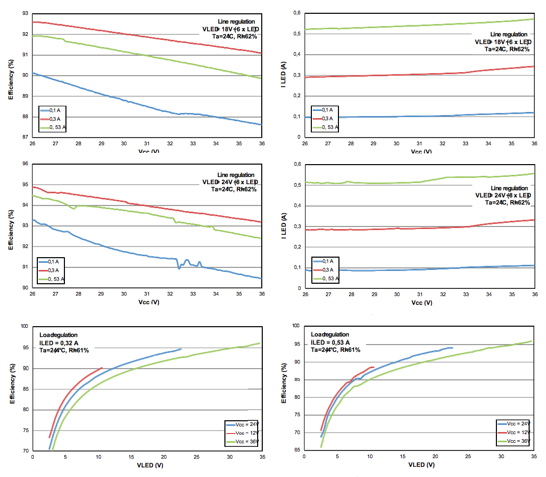
The TS19376 includes over temperature shutdown protection. Once the die temperature reaches 150°C the driver is disabled until the temperature drops below 115°C. This protection is useful to prevent burning of the module PCB. The driver module can be attached to an external heat sink with double-sided thermo-conductive tape (e.g. Bergquist Bond Ply). It is also possible to extend the driver module with EMI filtering, and reverse polarity protection (e.g. P-MOS switch), but this depends on the specific application. The driver module is populated on a 16x16 mm double-sided, 1 mm thick FR4 PCB. Conclusion The described LED driver has numerous applications from driving middle and high power LED arrays, to battery charging and much more where a constant current source is required. The number of LEDs in a serial string is determined from the minimum allowed input voltage (Vcc). As can be seen from the charts in Fig. 4, the closer VLED is to Vcc the higher the efficiency. For example for Vcc=12V, 3xLED in series is a good choice (VLEDF~3V). All measurements in Fig. 4 were acquired on automated measurement setup at room temperature. ----- Author: Valentin Kulikov, © FuturoLighting

Ad
Ad
Load more news
April 15 2024 11:45 am V22.4.27-1
Ad
Ad