

© linear technology
Application Notes |
High current rails demand a converter with control & supervision
The increasing complexity in large computing systems has exerted pressure on power supply manufactures to improve efficiency, accuracy and transient response.
More recently however, they are also demanding digital control for monitoring, settings and reporting. High efficiency is essential in distributed systems, where high step-down ratios from intermediate voltage busses are used to create local low voltage supplies sourcing high currents in order to minimize thermal concerns by poor conversion efficiencies. Host systems can have dozens of local voltage rails delivering a wide range of power levels. In datacom systems, for example, there can be as many as 50 point-of-load voltage rails some of which can have currents up to and exceeding a hundred amps. As a result, system designers would like to be able to easily monitor and adjust supply voltages, sequence, set operating voltage limits and read parameters like voltage, current and temperature as well as access detailed fault logging.
A popular way to control a high rail count system is over a digital communications bus. This is frequently referred to as “Digital Power” or “Power System Management (PSM)”, and enables designers to control, monitor and supervise dozens of rails in real time. The ability to digitally change power supply parameters significantly reduces time-to-market and down time by eliminating what would have historically required physical hardware, circuit, and/or system bill-of-material modifications.
Emerging PSM products tend to support configurability and monitoring via a 2-wire interface such as PMBus, which is an open standard I²C-based digital interface protocol. This provides a means for PSM products to seamlessly integrate with existing embedded systems and architectures, board mount controllers and intelligent platform management interface functions. For simplicity and ease of use, especially in the early stages of hardware development and testing, it is common to interact with PSM devices through a Graphical User Interface (GUI) running on a PC and through a USB-to-PMBus communications conversion tool commonly called a dongle.
PSM can be used to monitor the performance of a remote voltage regulator and report back on its health so that corrective action can be taken prior to it going out of specification or even a failure. PSM also allows users to act upon the information collected from the load and the system with the following benefits.
Faster Time-to-Market
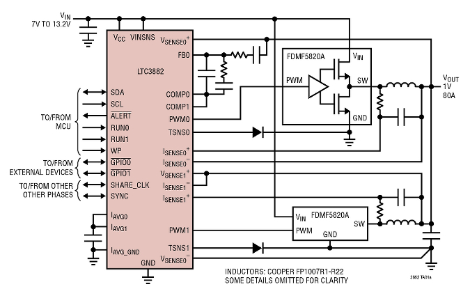 Figure 1. LTC3882 Typical Applications Schematic
Internal Architecture
In order to support high step-down ratios and fast load transient response, the LTC3882 utilizes a constant frequency, leading-edge modulation voltage mode architecture. This architecture is combined with a very low offset, high bandwidth voltage error amplifier and internal feed-forward compensation. Internal feed-forward compensation instantaneously adjusts the duty cycle for changes in input voltage, significantly reducing output overshoot or undershoot during a transient event.
Both channels feature remote output voltage sense to compensate for the voltage drop associated with long PCB traces. A separate control loop yields exceptional DC and dynamic multiphase load sharing when outputs are paralleled. Figure 2 shows the transient response of the figure 1 schematic with a 15A step-load. The maximum deviation from the nominal output voltage is less than 25mV.
Selection of Power Stages
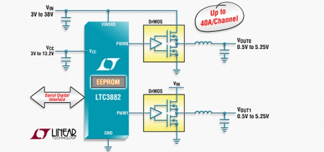
Each LTC3882 channel provide selectable PWM control protocols for interfacing to power stage designs that have 3.3V-compatible control inputs. The user can choose the optimum type of power stage for the design requirements: discrete FET drivers, DrMOS devices or power blocks. These can be mixed and matched on a per channel basis, allowing optimization of power subsystem partitioning, size and cost, according to the power delivery needs of each rail.
Leading-edge modulation affords fast, single-cycle response to output load steps and does not have a restriction on the minimum duty cycle. PWM output control pulses can become very small with this scheme for high step-down ratios, and the minimum on-time is normally limited by the power stage design, not the controller. For the most compact solution it is possible to use only ceramic output capacitors and the LTC3882 features programmable active voltage positioning (AVP), allowing further optimization of equivalent series resistance (ESR) and reduction in output capacitor size.
Depending on the needs of the application, peak efficiency or solution size can be prioritized by choosing an optimal operating frequency. The LTC3882’s programmable switching frequency of 250kHz to 1.25MHz supports optimization of inductor size and output current ripple. The LTC3882 can also serve as a shared PWM clock master or accept an external clock input for synchronization to another system time base.
Figure 1. LTC3882 Typical Applications Schematic
Internal Architecture
In order to support high step-down ratios and fast load transient response, the LTC3882 utilizes a constant frequency, leading-edge modulation voltage mode architecture. This architecture is combined with a very low offset, high bandwidth voltage error amplifier and internal feed-forward compensation. Internal feed-forward compensation instantaneously adjusts the duty cycle for changes in input voltage, significantly reducing output overshoot or undershoot during a transient event.
Both channels feature remote output voltage sense to compensate for the voltage drop associated with long PCB traces. A separate control loop yields exceptional DC and dynamic multiphase load sharing when outputs are paralleled. Figure 2 shows the transient response of the figure 1 schematic with a 15A step-load. The maximum deviation from the nominal output voltage is less than 25mV.
Selection of Power Stages
Each LTC3882 channel provide selectable PWM control protocols for interfacing to power stage designs that have 3.3V-compatible control inputs. The user can choose the optimum type of power stage for the design requirements: discrete FET drivers, DrMOS devices or power blocks. These can be mixed and matched on a per channel basis, allowing optimization of power subsystem partitioning, size and cost, according to the power delivery needs of each rail.
Leading-edge modulation affords fast, single-cycle response to output load steps and does not have a restriction on the minimum duty cycle. PWM output control pulses can become very small with this scheme for high step-down ratios, and the minimum on-time is normally limited by the power stage design, not the controller. For the most compact solution it is possible to use only ceramic output capacitors and the LTC3882 features programmable active voltage positioning (AVP), allowing further optimization of equivalent series resistance (ESR) and reduction in output capacitor size.
Depending on the needs of the application, peak efficiency or solution size can be prioritized by choosing an optimal operating frequency. The LTC3882’s programmable switching frequency of 250kHz to 1.25MHz supports optimization of inductor size and output current ripple. The LTC3882 can also serve as a shared PWM clock master or accept an external clock input for synchronization to another system time base.
- Change power parameters without re-working the PCB
- Perform quick system characterization, optimization and data mining
- Control power supply accuracy over time and temperature
- Margining to test FPGA tolerances
- Digital access to board level power diagnostics
- Monitor and pinpoint system wide power consumption
- Fault management/fault Logging
- Power consumption trends, detect fluctuations and changes over time
- Develop predictive analytics to minimize operating costs
- Make energy management decisions
Figure 1. LTC3882 Typical Applications Schematic
Internal Architecture
In order to support high step-down ratios and fast load transient response, the LTC3882 utilizes a constant frequency, leading-edge modulation voltage mode architecture. This architecture is combined with a very low offset, high bandwidth voltage error amplifier and internal feed-forward compensation. Internal feed-forward compensation instantaneously adjusts the duty cycle for changes in input voltage, significantly reducing output overshoot or undershoot during a transient event.
Both channels feature remote output voltage sense to compensate for the voltage drop associated with long PCB traces. A separate control loop yields exceptional DC and dynamic multiphase load sharing when outputs are paralleled. Figure 2 shows the transient response of the figure 1 schematic with a 15A step-load. The maximum deviation from the nominal output voltage is less than 25mV.
Selection of Power Stages
Each LTC3882 channel provide selectable PWM control protocols for interfacing to power stage designs that have 3.3V-compatible control inputs. The user can choose the optimum type of power stage for the design requirements: discrete FET drivers, DrMOS devices or power blocks. These can be mixed and matched on a per channel basis, allowing optimization of power subsystem partitioning, size and cost, according to the power delivery needs of each rail.
Leading-edge modulation affords fast, single-cycle response to output load steps and does not have a restriction on the minimum duty cycle. PWM output control pulses can become very small with this scheme for high step-down ratios, and the minimum on-time is normally limited by the power stage design, not the controller. For the most compact solution it is possible to use only ceramic output capacitors and the LTC3882 features programmable active voltage positioning (AVP), allowing further optimization of equivalent series resistance (ESR) and reduction in output capacitor size.
Depending on the needs of the application, peak efficiency or solution size can be prioritized by choosing an optimal operating frequency. The LTC3882’s programmable switching frequency of 250kHz to 1.25MHz supports optimization of inductor size and output current ripple. The LTC3882 can also serve as a shared PWM clock master or accept an external clock input for synchronization to another system time base.
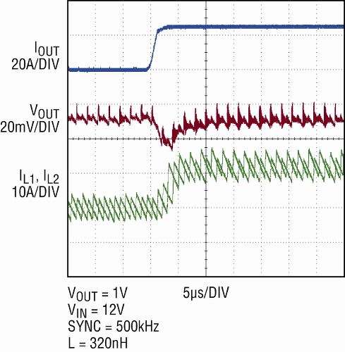
Low DCR Sensing for High Power At relatively high output currents, conversion efficiency must be maximized to limit heat production and minimize related cooling costs due to conduction losses. It is important to minimize the power loss in the current sense element to maximize efficiency because it continuously sees the full DC load current plus additional ripple current. The LTC3882 supports conventional sense resistor topologies as well as low DCR sense schemes that can produce only a few tens of millivolts. The fixed ramp voltage mode PWM architecture allows large signal control of the duty cycle and eliminates noise concerns that could be created by low DCR designs using current mode control schemes. The efficiency and power loss are shown in Figure 3 represented by the figure 1 schematic. The LTC3882 contains an optional digital output servo function. When enabled, the 16-bit ADC output for channel voltage is used to servo to the desired average output value. In this case, the converter has an impressive typical output error of only ±0.2% and a worse case error over temperature of ±0.5%. For multiphase single output operation, the LTC3882 features a separate current sharing loop that provides accurate load balancing, an improvement over conventional voltage mode converters. The output channels are designated as control masters or as slaves by pin strapping. The IAVG pin on the master channel provides a voltage analog of its instantaneous output current. A filter capacitor of 100pf to 200pf is added to this line, which is then routed to all slave phases. The slaves use this information and the primary COMP control voltage from the master to match their own output current to that of the master. Figure 4 shows that this matching is maintained dynamically through high speed load steps. Accurate telemetry The LTC3882 monitors critical supply parameters with an internal 16-bit ADC. Digital readback via PMBus is available for input and output voltages, output currents, duty cycles and temperatures. The LTC3882 tracks, maintains and provides peak values for these parameters. Beyond basic supply parameter telemetry, the LTC3882 can report a wide range of internal and external status information to the system host over the PMBus. Fast Programmable Fault Response Faults can be detected and communicated using a shared fault bus between LTC3882s as well as other Linear Technology PSM family members, such as the LTC3880. The LTC3882 provides a standard open-drain ALERT output for notification of a wide range of fault conditions to the bus host. The LTC3882 implements high speed, low level hardware responses to critical faults to protect the power stage and downstream system load. PMBus commands can then be used to configure higher-level responses, mask faults to the system, and determine which faults are propagated to the shared fault bus. This provides flexibility in dynamically managing fault handling at the system level, even after hardware has been designed and fabricated. The LTC3882 includes extensive logging capability that records the state of converter operating conditions immediately prior to a fault. This log can be enabled and stored to internal EEPROM to provide a black box recorder function for in-system diagnosis or subsequent remote debugging of abnormal events. Advantage of PSM There are many reasons to consider use of a PSM controller. PMBus commands can be issued to the LTC3882 to set output voltage, margin voltages, switching frequency, output on/off sequencing and other operating parameters. In total, the LTC3882 supports over 100 PMBus commands, both standard and custom. A principal benefit of this programmability is reduced design cost and faster time to market. Once a fundamental hardware macro design is complete, many variations can quickly be created, brought to operation and verified as needed by simply adjusting digitally programmable parameters inside the LTC3882 controller. Adjustments can continue beyond production release as needed, including fully synchronized re-sequencing/retiming of power rails. Combined with optional external resistor programming of key supply parameters, this kind of flexibility can avoid risky, costly PCB spins or hand-wired modifications due to last-minute changes in requirements or evolving system use. Final configurations can be readily stored on its internal EEPROM using a variety of means, including custom factory programming. Once a configuration is stored, the controller powers up autonomously to that state without burdening the host for additional programming. However, even after a final EEPROM configuration is loaded, optional external programming resistors can be used to modify a few key operating parameters such as the output voltage, frequency and phase assignments. Once designed, the multiple addressing schemes supported by the LTC3882 allow the system to communicate with devices globally or selectively at the rail, device or individual channel level, depending on control and monitoring requirements. PMBus then facilitates sophisticated high level system operations, such as energy-efficient application load balancing in high current requirements. These functions would simply not be cost-effective or even possible with conventional power supply components in large systems. Conclusion PSM is a way for system designers to control power supplies with an existing system host processor or with a simple PC connection. This capability is valuable during the development and debug stage enabling designers to get their systems up and running quickly with the ability to control and adjust supply voltages, limits and sequencing without the need for physical hardware, circuit, and/or system bill-of-material modifications. For high rail count systems, some of which require high current and for OEM’s that want to take control of their power systems, PSM is a simple, practical and powerful tool. ----- Author: Bruce Haug, Senior Product Marketing Engineer, Power Products at © Linear Technology CorporationFigure 2. Transient Response of Figure 1 Circuit -----
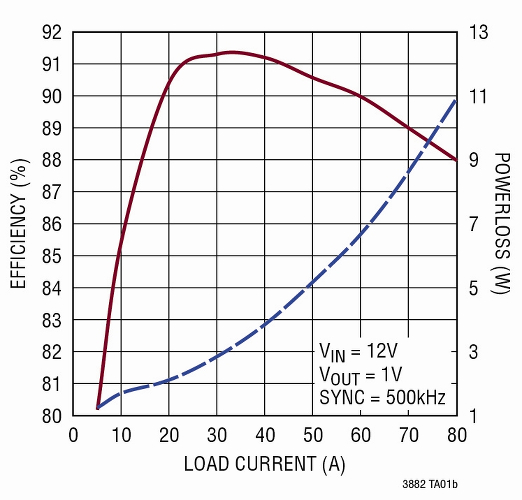
Figure 3. Efficiency and Power Loss Curves for a 12V input to 1V Output -----
Figure 4. Dynamic Load Balancing During an Output Transient ----- Images have zoom

.png)