© carabiner dreamstime.com
Application Notes |
Part 3: Design considerations of the switching power components
In general, higher switching frequency means smaller size output filter components L and CO. As a result, the size and cost of the power supply can be reduced.
[chapter-index=Index Head link-to=33057,33080]Application Note: P281[/chapter-index]Switching Frequency Optimization
Higher bandwidth can also improve load transient response. However, higher switching frequency also means higher AC-related power loss, which requires larger board space or a heat sink to limit the thermal stress. Currently, for ≥10A output current applications, most step-down sup-plies operate in the range of 100kHz to 1MHz ~ 2MHz. For < 10A load current, the switching frequency can be up to several MHz. The optimum frequency for each design is a result of careful trade-offs in size, cost, efficiency and other performance parameters.
Output Inductor Selection
In a synchronous buck converter, the inductor peak-to-peak ripple current can be calculated as:
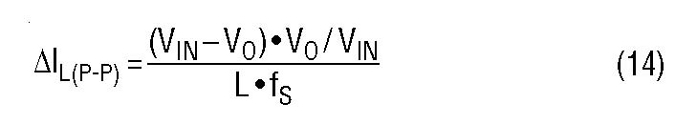 With a given switching frequency, a low inductance gives large ripple current and results in large output ripple voltage. Large ripple current also increases MOSFET RMS current and conduction losses. On the other hand, high inductance means large inductor size and possible high inductor DCR and conduction losses. In general, 10% ~ 60% peak-to-peak ripple current is chosen over the maximum DC current ratio when selecting an inductor. The inductor vendors usually specify the DCR, RMS (heating) current and saturation current ratings. It is important to design the maximum DC current and peak current of the inductor within the vendor’s maximum ratings.
Power MOSFET Selection
When selecting a MOSFET for a buck converter, first make sure its maximum VDS rating is higher than the supply VIN(MAX) with sufficient margin. However, do not select a FET with an excessively high voltage rating. For example, for a 16VIN(MAX) supply, a 25V or 30V rated FET is a good fit. A 60V rated FET can be excessive, because the FET on-resistance usually increases with rated voltage. Next, the FET’s on-resistance RDS(ON) and gate charge QG (or QGD) are two most critical parameters.
There is usually a trade-off between the gate charge QG and on-resistance RDS(ON). In general, a FET with small silicon die size has low QG but high on-resistance RDS(ON), while a FET with a large silicon die has low RDS(ON) but large QG. In a buck converter, the top MOSFET Q1 takes both conduction loss and AC switching loss. A low QG FET is usually needed for Q1, especially in applications with low output voltage and small duty cycle. The lower side synchronous FET Q2 has small AC loss because it is usually turned on or off when its VDS voltage is near zero. In this case, low RDS(ON) is more important than QG for synchronous FET Q2. When a single FET cannot handle the total power, several MOSFETs can be used in parallel.
Input and Output Capacitor Selection
First, the capacitors should be selected with sufficient voltage derating.
The input capacitor of a buck converter has pulsating switching current with large ripple. Therefore, the input capacitor should be selected with sufficient RMS ripple current rating to ensure its lifetime. Aluminum electrolytic capacitors and low ESR ceramic capacitors are usually used in parallel at the input.
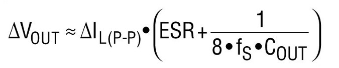
The output capacitor determines not only the output voltage ripple, but also the load transient performance. The output voltage ripple can be calculated by Equation (15). For high performance applications, both the ESR and total capacitance are important to minimize output ripple voltage and to optimize load transient response. Usually, low ESR tantalum, low ESR polymer capacitors and multilayer ceramic capacitors (MLCC) are good choices.
With a given switching frequency, a low inductance gives large ripple current and results in large output ripple voltage. Large ripple current also increases MOSFET RMS current and conduction losses. On the other hand, high inductance means large inductor size and possible high inductor DCR and conduction losses. In general, 10% ~ 60% peak-to-peak ripple current is chosen over the maximum DC current ratio when selecting an inductor. The inductor vendors usually specify the DCR, RMS (heating) current and saturation current ratings. It is important to design the maximum DC current and peak current of the inductor within the vendor’s maximum ratings.
Power MOSFET Selection
When selecting a MOSFET for a buck converter, first make sure its maximum VDS rating is higher than the supply VIN(MAX) with sufficient margin. However, do not select a FET with an excessively high voltage rating. For example, for a 16VIN(MAX) supply, a 25V or 30V rated FET is a good fit. A 60V rated FET can be excessive, because the FET on-resistance usually increases with rated voltage. Next, the FET’s on-resistance RDS(ON) and gate charge QG (or QGD) are two most critical parameters.
There is usually a trade-off between the gate charge QG and on-resistance RDS(ON). In general, a FET with small silicon die size has low QG but high on-resistance RDS(ON), while a FET with a large silicon die has low RDS(ON) but large QG. In a buck converter, the top MOSFET Q1 takes both conduction loss and AC switching loss. A low QG FET is usually needed for Q1, especially in applications with low output voltage and small duty cycle. The lower side synchronous FET Q2 has small AC loss because it is usually turned on or off when its VDS voltage is near zero. In this case, low RDS(ON) is more important than QG for synchronous FET Q2. When a single FET cannot handle the total power, several MOSFETs can be used in parallel.
Input and Output Capacitor Selection
First, the capacitors should be selected with sufficient voltage derating.
The input capacitor of a buck converter has pulsating switching current with large ripple. Therefore, the input capacitor should be selected with sufficient RMS ripple current rating to ensure its lifetime. Aluminum electrolytic capacitors and low ESR ceramic capacitors are usually used in parallel at the input.
The output capacitor determines not only the output voltage ripple, but also the load transient performance. The output voltage ripple can be calculated by Equation (15). For high performance applications, both the ESR and total capacitance are important to minimize output ripple voltage and to optimize load transient response. Usually, low ESR tantalum, low ESR polymer capacitors and multilayer ceramic capacitors (MLCC) are good choices.
 Close the Feedback Regulation Loop
There is another important design stage for a switching mode supply—closing the regulation loop with a negative feedback control scheme. This is usually a much more challenging task than using an LR or LDO. It requires good understanding of loop behavior and compensation design to optimize dynamic performance with a stable loop.
Small Signal Model of the Buck Converter
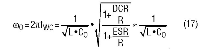
As explained above, a switching converter changes its operation mode as a function of the switch ON or OFF state. It is a discrete and nonlinear system. To analyze the feedback loop with the linear control method, linear small signal modeling is needed. Because of the output L-C filter, the linear small signal transfer function of duty cycle D to output VO is actually a second-order system with two poles and one zero, as shown in Equation (16). There are double poles located at the resonant frequency of the output inductor and capacitor. There is a zero determined by the output capacitance and the capacitor ESR.
Close the Feedback Regulation Loop
There is another important design stage for a switching mode supply—closing the regulation loop with a negative feedback control scheme. This is usually a much more challenging task than using an LR or LDO. It requires good understanding of loop behavior and compensation design to optimize dynamic performance with a stable loop.
Small Signal Model of the Buck Converter
As explained above, a switching converter changes its operation mode as a function of the switch ON or OFF state. It is a discrete and nonlinear system. To analyze the feedback loop with the linear control method, linear small signal modeling is needed. Because of the output L-C filter, the linear small signal transfer function of duty cycle D to output VO is actually a second-order system with two poles and one zero, as shown in Equation (16). There are double poles located at the resonant frequency of the output inductor and capacitor. There is a zero determined by the output capacitance and the capacitor ESR.
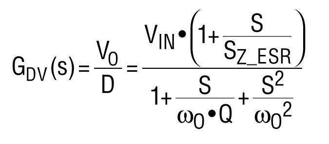 Where, SZ_ESR = 2πfZ_ESR = 1 / ESR • CO ,
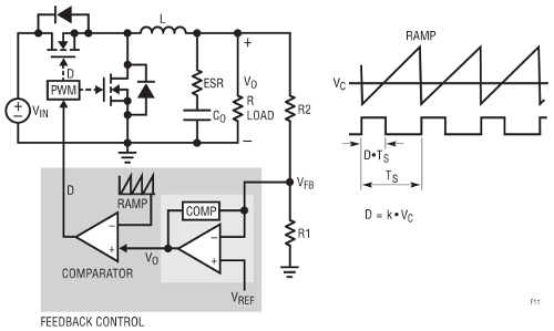
 Voltage Mode Control vs. Current Mode Control
The output voltage can be regulated by a closed loop system shown in Figure 11. For example, when the output voltage increases, the feedback voltage VFB increases and the output of the negative feedback error amplifier decreases. So the duty cycle decreases. As a result, the output voltage is pulled back to make VFB = VREF. The compensation network of the error op amp can be a type I, type II or type III feedback amplifier network. There is only one control loop to regulate the output. This scheme is referred to as voltage mode control. Linear Technology’s LTC3775 and LTC3861 are typical voltage mode buck controllers.
Voltage Mode Control vs. Current Mode Control
The output voltage can be regulated by a closed loop system shown in Figure 11. For example, when the output voltage increases, the feedback voltage VFB increases and the output of the negative feedback error amplifier decreases. So the duty cycle decreases. As a result, the output voltage is pulled back to make VFB = VREF. The compensation network of the error op amp can be a type I, type II or type III feedback amplifier network. There is only one control loop to regulate the output. This scheme is referred to as voltage mode control. Linear Technology’s LTC3775 and LTC3861 are typical voltage mode buck controllers.
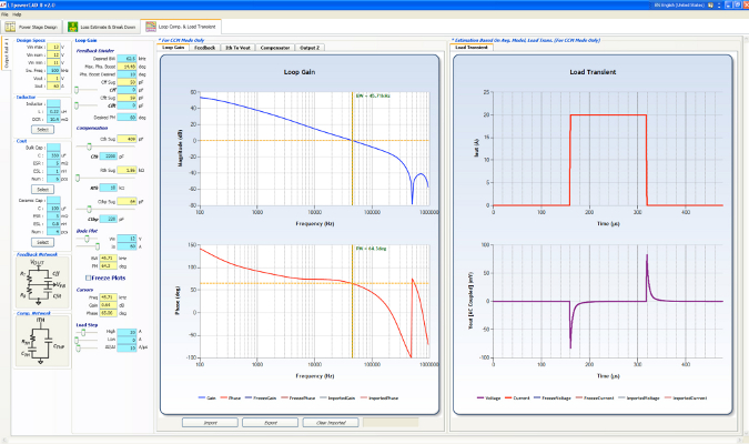 Figure 16. LTpowerCAD Design Tool Provides an Easy Way to Optimize the Loop Compensation and Load Transient Response (3-Phase, Single-Output LTC3829 Buck Converter Example).
PolyPhase Buck Converter for High Current Applications
As data processing systems become faster and larger, their processor and memory units demand more current at ever decreasing voltages. At these high currents, the demands on power supplies are multiplied. In recent years, PolyPhase (multiphase) synchronous buck converters have been widely used for high current, low voltage power supply solutions, due to their high efficiency and even thermal distribution. Besides, with interleaved multiple buck converter phases, the ripple current on both input and output sides can be significantly reduced, resulting in reduction of input and output capacitors and related board space and cost.
In PolyPhase buck converters, precise current sensing and sharing become extremely important. Good current sharing ensures even thermal distribution and high system reliability. Because of their inherent current sharing capability in steady state and during transients, current mode-controlled bucks are usually preferred. Linear Technology’s LTC3856 and LTC3829 are typical PolyPhase buck controllers with precise current sensing and sharing. Multiple controllers can be connected in a daisy chain fashion for 2-, 3-, 4-, 6- and 12-phase systems with output current from 20A to over 200A.
Figure 16. LTpowerCAD Design Tool Provides an Easy Way to Optimize the Loop Compensation and Load Transient Response (3-Phase, Single-Output LTC3829 Buck Converter Example).
PolyPhase Buck Converter for High Current Applications
As data processing systems become faster and larger, their processor and memory units demand more current at ever decreasing voltages. At these high currents, the demands on power supplies are multiplied. In recent years, PolyPhase (multiphase) synchronous buck converters have been widely used for high current, low voltage power supply solutions, due to their high efficiency and even thermal distribution. Besides, with interleaved multiple buck converter phases, the ripple current on both input and output sides can be significantly reduced, resulting in reduction of input and output capacitors and related board space and cost.
In PolyPhase buck converters, precise current sensing and sharing become extremely important. Good current sharing ensures even thermal distribution and high system reliability. Because of their inherent current sharing capability in steady state and during transients, current mode-controlled bucks are usually preferred. Linear Technology’s LTC3856 and LTC3829 are typical PolyPhase buck controllers with precise current sensing and sharing. Multiple controllers can be connected in a daisy chain fashion for 2-, 3-, 4-, 6- and 12-phase systems with output current from 20A to over 200A.
With a given switching frequency, a low inductance gives large ripple current and results in large output ripple voltage. Large ripple current also increases MOSFET RMS current and conduction losses. On the other hand, high inductance means large inductor size and possible high inductor DCR and conduction losses. In general, 10% ~ 60% peak-to-peak ripple current is chosen over the maximum DC current ratio when selecting an inductor. The inductor vendors usually specify the DCR, RMS (heating) current and saturation current ratings. It is important to design the maximum DC current and peak current of the inductor within the vendor’s maximum ratings.
Power MOSFET Selection
When selecting a MOSFET for a buck converter, first make sure its maximum VDS rating is higher than the supply VIN(MAX) with sufficient margin. However, do not select a FET with an excessively high voltage rating. For example, for a 16VIN(MAX) supply, a 25V or 30V rated FET is a good fit. A 60V rated FET can be excessive, because the FET on-resistance usually increases with rated voltage. Next, the FET’s on-resistance RDS(ON) and gate charge QG (or QGD) are two most critical parameters.
There is usually a trade-off between the gate charge QG and on-resistance RDS(ON). In general, a FET with small silicon die size has low QG but high on-resistance RDS(ON), while a FET with a large silicon die has low RDS(ON) but large QG. In a buck converter, the top MOSFET Q1 takes both conduction loss and AC switching loss. A low QG FET is usually needed for Q1, especially in applications with low output voltage and small duty cycle. The lower side synchronous FET Q2 has small AC loss because it is usually turned on or off when its VDS voltage is near zero. In this case, low RDS(ON) is more important than QG for synchronous FET Q2. When a single FET cannot handle the total power, several MOSFETs can be used in parallel.
Input and Output Capacitor Selection
First, the capacitors should be selected with sufficient voltage derating.
The input capacitor of a buck converter has pulsating switching current with large ripple. Therefore, the input capacitor should be selected with sufficient RMS ripple current rating to ensure its lifetime. Aluminum electrolytic capacitors and low ESR ceramic capacitors are usually used in parallel at the input.
The output capacitor determines not only the output voltage ripple, but also the load transient performance. The output voltage ripple can be calculated by Equation (15). For high performance applications, both the ESR and total capacitance are important to minimize output ripple voltage and to optimize load transient response. Usually, low ESR tantalum, low ESR polymer capacitors and multilayer ceramic capacitors (MLCC) are good choices.
Close the Feedback Regulation Loop
There is another important design stage for a switching mode supply—closing the regulation loop with a negative feedback control scheme. This is usually a much more challenging task than using an LR or LDO. It requires good understanding of loop behavior and compensation design to optimize dynamic performance with a stable loop.
Small Signal Model of the Buck Converter
As explained above, a switching converter changes its operation mode as a function of the switch ON or OFF state. It is a discrete and nonlinear system. To analyze the feedback loop with the linear control method, linear small signal modeling is needed. Because of the output L-C filter, the linear small signal transfer function of duty cycle D to output VO is actually a second-order system with two poles and one zero, as shown in Equation (16). There are double poles located at the resonant frequency of the output inductor and capacitor. There is a zero determined by the output capacitance and the capacitor ESR.
Where, SZ_ESR = 2πfZ_ESR = 1 / ESR • CO ,
Voltage Mode Control vs. Current Mode Control
The output voltage can be regulated by a closed loop system shown in Figure 11. For example, when the output voltage increases, the feedback voltage VFB increases and the output of the negative feedback error amplifier decreases. So the duty cycle decreases. As a result, the output voltage is pulled back to make VFB = VREF. The compensation network of the error op amp can be a type I, type II or type III feedback amplifier network. There is only one control loop to regulate the output. This scheme is referred to as voltage mode control. Linear Technology’s LTC3775 and LTC3861 are typical voltage mode buck controllers.
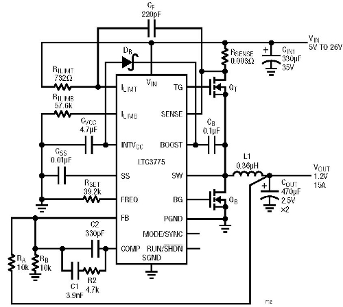
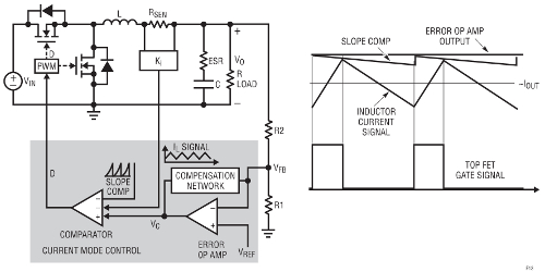
Figure 12 shows a 5V to 26V input, 1.2V/15A output synchronous buck supply using the LTC3775 voltage mode buck controller. Due to the LTC3775’s leading-edge PWM modulation architecture and very low (30ns) minimum on-time, the supply operates well for applications that convert a high voltage automotive or industrial power supply down to the 1.2V low voltage required by today’s microprocessors and programmable logic chips. High power applications require multiphase buck converters with current sharing. With voltage mode control, an additional current sharing loop is required to balance current among parallel buck channels. A typical current sharing method for voltage mode control is the master-slave method. The LTC3861 is such a PolyPhase® voltage mode controller. Its very low, ±1.25mV, current sense offset makes current sharing between paralleled phases very accurate to balance the thermal stress. Current mode control uses two feedback loops: an outer voltage loop similar to the control loop of voltage mode-controlled converters, and an inner current loop that feeds back the current signal into the control loop. Figure 13 shows the conceptual block diagram of a peak current mode control buck converter that directly senses the output inductor current. With current mode control, the inductor current is determined by the error op amp output voltage. The inductor becomes a current source. Therefore, the transfer function from op amp output, VC, to supply output voltage VO becomes a single pole system. This makes loop compensation much easier. The control loop compensation has less dependency on the output capacitor ESR zero, so it is possible to use all ceramic output capacitors. There are many other benefits from current mode control. As shown in Figure 13, since the peak inductor current is limited by the op amp VC in a cycle-by-cycle fashion, the current mode-controlled system provides a more accurate and faster current limit under overload conditions. The in-rush inductor current is well controlled during start-up, too. Also, the inductor current does not change quickly when the input voltage changes, so the supply has good line transient performance. When multiple converters are paralleled, with current mode control, it is also very easy to share current among supplies, which is important for reliable high current applications using PolyPhase buck converters. In general, a current mode-controlled converter is more reliable than a voltage mode-controlled converter. The current mode control scheme solution needs to sense the current precisely. The current sensing signal is usually a small signal at a level of tens of millivolts that is sensitive to switching noise. Therefore, proper and careful PCB layout is needed. The current loop can be closed by sensing the inductor current through a sensing resistor, the inductor DCR voltage drop, or the MOSFET conduction voltage drop. Typical current mode controllers include Linear Technology’s LTC3851A and LTC3855. Constant Frequency vs. Constant On-Time Control Typical voltage mode and current mode schemes in the Voltage Mode Control vs. Current Mode Control section have constant switching frequency generated by controller internal clocks. These constant switching frequency controllers can be easily synchronized, an important feature for high current, PolyPhase buck controllers. However, if the load step-up transient occurs just after the control FET Q1 gate is turned off, the converter must wait the entire Q1 off-time until the next cycle to respond to the transient. In applications with small duty cycles, the worst-case delay is close to one switching cycle. In such low duty cycle applications, constant on-time valley current mode control has shorter latency to respond to load step-up transients. In steady state operation, the switching frequency of constant on-time buck converters is nearly fixed. In the event of a transient, the switching frequency can vary quickly to speed up the transient response. As a result, the supply has improved transient performance and output capacitance and its related cost can be reduced. However, with constant on-time control, the switching frequency may vary with line or load. The LTC3833 is a valley current mode buck controller with a more sophisticated controlled-on-time architecture—a variant of the constant on-time control architecture with the distinction that the on-time is controlled so that the switching frequency remains constant over steady stage conditions under line and load. With this architecture, the LTC3833 controller has 20ns minimum on-time and allows step-down applications from up to 38VIN to 0.6VO.Figure 11. Block Diagram of a Voltage Mode-Controlled Buck Converter
Figure 12. The LTC3775 Voltage Mode Synchronous Buck Supply Offers a High Step-Down Ratio
Figure 13. Block Diagram of a Current Mode-Controlled Buck Converter
The controller can be synchronized to an external clock in the 200kHz to 2MHz frequency range. Figure 14 shows a typical LTC3833 supply with 4.5V to 14V input and 1.5V/20A output. Figure 15 shows that the supply can respond quickly to sudden, high slew rate load transients. During the load step-up transient, the switching frequency increases to provide faster transient response. During the load step-down transient, the duty-cycle drops to zero. Therefore only the output inductor limits the current slew rate. In addition to the LTC3833, for multiple outputs or PolyPhase applications, the LTC3838 and LTC3839 controllers provide fast transient, multiphase solutions. Loop Bandwidth and Stability A well-designed SMPS is quiet, both electrically and acoustically. This is not the case with an undercompensated system, which tends to be unstable. Typical symptoms of an undercompensated power supply include: audible noise from the magnetic components or ceramic capacitors, jitter in the switching waveforms, oscillation of output voltage, and so on. An overcompensated system can be very stable and quiet, but at the cost of a slow transient response. Such a system has a loop crossover frequency at very low frequencies, typically below 10kHz. Slow transient response designs require excessive output capacitance to meet transient regulation requirements, increasing the overall supply cost and size. An optimum loop compensation design is stable and quiet, but is not overcompensated, so it also has a fast response to minimize output capacitance. There are numerous articles that discuss how to optimize loop compensation networks for both voltage mode-controlled and current mode-controlled SMPS. Small signal modeling and loop compensation design can be difficult for inexperienced power supply designers. Linear Technology’s LTpowerCAD™ design tool handles the complicated equations and makes loop compensation a much simpler task. The LTspice® simulation tool integrates all of Linear Technology’s part models and provides additional time domain simulations to optimize the design. However, bench test/verification of loop stability and transient performance is usually necessary in the prototype stage. In general, the performance of the closed voltage regulation loop is evaluated by two important values: the loop bandwidth and the loop stability margin. The loop bandwidth is quantified by the crossover frequency fC, at which the loop gain T(s) equals one (0dB). The loop stability margin is typically quantified by the phase margin or gain margin. The loop phase margin Φm is defined as the difference between the overall T(s) phase delay and –180° at the crossover frequency. The gain margin is defined by the difference between T(s) gain and 0dB at the frequency where overall T(s) phase equals –180°. For a buck converter, typically 45-degree phase margin and 10dB gain margin is considered sufficient. Figure 16 shows a typical Bode plot of loop gain for a current mode LTC3829 12VIN to 1VO/60A 3-phase buck converter. In this example, the crossover frequency is 45kHz and the phase margin is 64 degrees. The gain margin is close to 20dB.Zoom image: Figure 14. Fast, Controlled-On-Time Current Mode Supply Using the LTC3833
Zoom image: Figure 15. LTC3833 Supply Offers Fast Response During Rapid Load Step Transients
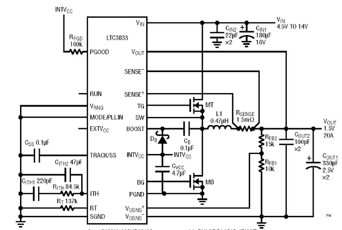
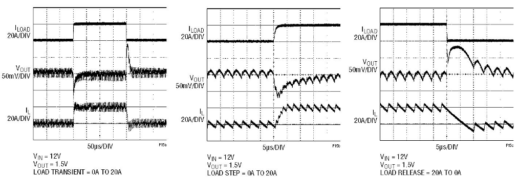 Figure 16. LTpowerCAD Design Tool Provides an Easy Way to Optimize the Loop Compensation and Load Transient Response (3-Phase, Single-Output LTC3829 Buck Converter Example).
PolyPhase Buck Converter for High Current Applications
As data processing systems become faster and larger, their processor and memory units demand more current at ever decreasing voltages. At these high currents, the demands on power supplies are multiplied. In recent years, PolyPhase (multiphase) synchronous buck converters have been widely used for high current, low voltage power supply solutions, due to their high efficiency and even thermal distribution. Besides, with interleaved multiple buck converter phases, the ripple current on both input and output sides can be significantly reduced, resulting in reduction of input and output capacitors and related board space and cost.
In PolyPhase buck converters, precise current sensing and sharing become extremely important. Good current sharing ensures even thermal distribution and high system reliability. Because of their inherent current sharing capability in steady state and during transients, current mode-controlled bucks are usually preferred. Linear Technology’s LTC3856 and LTC3829 are typical PolyPhase buck controllers with precise current sensing and sharing. Multiple controllers can be connected in a daisy chain fashion for 2-, 3-, 4-, 6- and 12-phase systems with output current from 20A to over 200A.
Figure 16. LTpowerCAD Design Tool Provides an Easy Way to Optimize the Loop Compensation and Load Transient Response (3-Phase, Single-Output LTC3829 Buck Converter Example).
PolyPhase Buck Converter for High Current Applications
As data processing systems become faster and larger, their processor and memory units demand more current at ever decreasing voltages. At these high currents, the demands on power supplies are multiplied. In recent years, PolyPhase (multiphase) synchronous buck converters have been widely used for high current, low voltage power supply solutions, due to their high efficiency and even thermal distribution. Besides, with interleaved multiple buck converter phases, the ripple current on both input and output sides can be significantly reduced, resulting in reduction of input and output capacitors and related board space and cost.
In PolyPhase buck converters, precise current sensing and sharing become extremely important. Good current sharing ensures even thermal distribution and high system reliability. Because of their inherent current sharing capability in steady state and during transients, current mode-controlled bucks are usually preferred. Linear Technology’s LTC3856 and LTC3829 are typical PolyPhase buck controllers with precise current sensing and sharing. Multiple controllers can be connected in a daisy chain fashion for 2-, 3-, 4-, 6- and 12-phase systems with output current from 20A to over 200A.
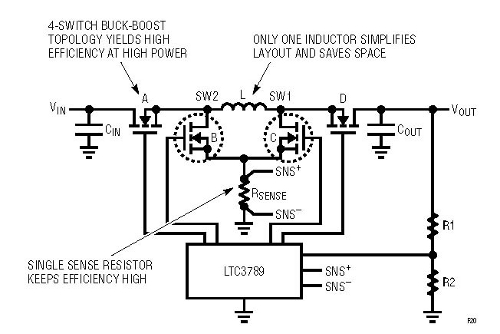
Other Requirements of a High Performance Controller Many other important features are required of a high performance buck controller. Soft-start is usually needed to control the inrush current during start-up. Overcurrent limit and short-circuit latchoff can protect the supply when the output is overloaded or shorted. Overvoltage protection safeguards the expensive load devices in the system. To minimize system EMI noise, sometimes the controller must be synchronized to an external clock signal. For low voltage, high current applications, remote differential voltage sensing compensates for the PCB resistance voltage drop and accurately regulates output voltage at the remote load. In a complicated system with many output voltage rails, sequencing and tracking among different voltage rails is also necessary. PCB Layout Component selection and schematic design is only half of the supply design process. Proper PCB layout of a switching supply design is always critical. In fact, its importance cannot be overstated. Good layout design optimizes supply efficiency, alleviates thermal stress, and most importantly, minimizes noise and interactions among traces and components. To achieve this, it is important for the designer to understand the current conduction paths and signal flows in the switching power supply. It usually requires significant effort to gain the necessary experience. See Linear Technology Application Note 136 for detailed discussions. Selection of Various Solutions – Discrete, Monolithic and Integrated Supplies At the integration level, system engineers can decide whether to choose a discrete, monolithic or fully integrated power module solution. Figure 18 shows examples of discrete and power module solutions for typical point-of-load supply applications. The discrete solution uses a controller IC, external MOSFETs and passive components to build the power supply on the system board. A major reason to choose a discrete solution is low component bill of materials (BOM) cost. However, this requires good power supply design skills and relatively long development time. A monolithic solution uses an IC with integrated power MOSFETs to further reduce the solution size and component count. It requires similar design skills and time. A fully integrated power module solution can significantly reduce design effort, development time, solution size and design risk, but usually with a higher component BOM cost. Other Basic Non-isolated DC/DC SMPS Topologies This application note uses buck converters as a simple ex-ample to demonstrate the design considerations of SMPS. However, there are at least five other basic non-isolated converter topologies (boost, buck/boost, Cuk, SEPIC and Zeta converters) and at least five basic isolated converter topologies (flyback, forward, push-pull, half-bridge and full-bridge), which are not covered in this application note. Each topology has unique properties that make it suited for specific applications. Figure 19 shows simplified schematics for the other non-isolated SMPS topologies. There are other non-isolated SMPS topologies, which are combinations of the basic topologies. For example, Figure 20 shows a high efficiency, 4-switch synchronous buck/boost converter based on the LTC3789 current mode controller. It can operate with input voltages below, equal, or above the output voltage. For example, the input can be in the range of 5V to 36V, and the output can be a regulated 12V. This topology is a combination of a synchronous buck converter and a synchronous boost converter, sharing a single inductor. When VIN > VOUT, switches A and B operate as an active synchronous buck converter, while the switch C is always off and switch D is always on. When VIN < VOUT, switches C and D operate as an active synchronous boost converter, while switch A is always on and switch B is always off. When VIN is close to VOUT, all four switches operate actively. As a result, this converter can be very efficient, with up to 98% efficiency for a typical 12V output application. The LT8705 controller further extends the input voltage range up to 80V. To simplify the design and increase power density, the LTM4605, LTM4607 and LTM4609 further integrate a complicated buck/boost converter into a high density, easy-to-use power module. They can be easily paralleled with load sharing for high power applications. [chapter-index=Index Head link-to=33057,33080]Application Note: P281[/chapter-index]SUMMARY In summary, linear regulators are simple and easy to use. Since their series regulation transistors are operated in a linear mode, supply efficiency is usually low when output voltage is much lower than input voltage. In general, linear regulators (or LDOs) have low voltage ripple and fast transient response. On the other hand, SMPS operate the transistor as a switch, and therefore are usually much more efficient than linear regulators. However, the design and optimization of SMPS are more challenging and require more background and experience. Each solution has its own advantages and drawbacks for specific applications.Zoom image: Figure 17. A 3-Phase, Single VO High Current Buck Converter Using the LTC3829
Figure 18. Examples of (a) a Discrete 12VIN to 3.3V/10A LTC3778 Supply; (b) a Fully Integrated 16VIN, Dual 13A or Single 26A LTM4620 µModule® Step-Down Regulator
Figure 19. Other Basic Non-isolated DC/DC Converter Topologies
Zoom image: Figure 20. High Efficiency 4-Switch Buck-Boost Converter Operates with Input Voltage Below, Equal or Above the Output Voltage / © Linear Technology