
© dmitry naumov dreamstime.com
Application Notes |
Part 2: Switching Mode power supply basics
Why Use a Switching Mode Supply? A quick answer is high efficiency. In an SMPS, the transistors are operated in switching mode instead of linear mode.
[chapter-index=Index Head link-to=33057,33082]Application Note: P281[/chapter-index]This means that when the transistor is on and conducting current, the voltage drop across its power path is minimal. When the transistor is off and blocking high voltage, there is almost no current through its power path. So the semiconductor transistor is like an ideal switch.
The power loss in the transistor is therefore minimized. High efficiency, low power dissipation and high power density (small size) are the main reasons for designers to use SMPS instead of linear regulators or LDOs, especially in high current applications. For example, nowadays a 12VIN, 3.3VOUT switching mode synchronous buck step-down supply can usually achieve >90% efficiency vs. less than 27.5% from a linear regulator. This means a power loss or size reduction of at least eight times.
The Most Popular Switching Supply—the Buck Converter
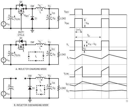
Figure 8 shows the simplest and most popular switching regulator, the buck DC/DC converter. It has two operating modes, depending on if the transistor Q1 is turned on or off. To simplify the discussion, all the power devices are assumed to be ideal. When switch (transistor) Q1 is turned on, the switching node voltage VSW = VIN and inductor L current is being charged up by (VIN – VO). Figure 8(a) shows the equivalent circuit in this inductor-charging mode. When switch Q1 is turned off, inductor current goes through the freewheeling diode D1, as shown in Figure 8(b). The switching node voltage VSW = 0V and inductor L current is discharged by the VO load. Since the ideal inductor cannot have DC voltage in the steady state, the average output voltage VO can be given as:
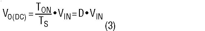
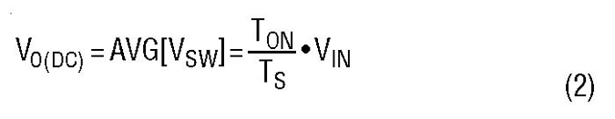 Where TON is the on-time interval within the switching period TS. If the ratio of TON/TS is defined as duty cycle D, the output voltage VO is:
 When the filter inductor L and output capacitor CO values are sufficiently high, the output voltage VO is a DC voltage with only mV ripple. In this case, for a 12V input buck supply, conceptually, a 27.5% duty cycle provides a 3.3V output voltage.
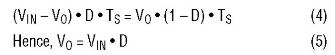 Equation (5) is the same as equation (3). The same volt-second balance approach can be used for other DC/DC topologies to derive the duty cycle vs. VIN and VO equations.
Power Losses in a Buck Converter
- DC Conduction Losses
With ideal components (zero voltage drop in the ON state and zero switching loss), an ideal buck converter is 100% efficient. In reality, power dissipation is always associated with every power component. There are two types of losses in an SMPS: DC conduction losses and AC switching losses.
The conduction losses of a buck converter primarily result from voltage drops across transistor Q1, diode D1 and inductor L when they conduct current. To simplify the discussion, the AC ripple of inductor current is neglected in the following conduction loss calculation. If a MOSFET is used as the power transistor, the conduction loss of the MOSFET equals IO2 • RDS(ON) • D, where RDS(ON) is the on-resistance of MOSFET Q1. The conduction power loss of the diode equals IO • VD • (1 – D), where VD is the forward voltage drop of the diode D1. The conduction loss of the inductor equals IO2 • RDCR, where RDCR is the copper resistance of the inductor winding. Therefore, the conduction loss of the buck converter is approximately:
Equation (5) is the same as equation (3). The same volt-second balance approach can be used for other DC/DC topologies to derive the duty cycle vs. VIN and VO equations.
Power Losses in a Buck Converter
- DC Conduction Losses
With ideal components (zero voltage drop in the ON state and zero switching loss), an ideal buck converter is 100% efficient. In reality, power dissipation is always associated with every power component. There are two types of losses in an SMPS: DC conduction losses and AC switching losses.
The conduction losses of a buck converter primarily result from voltage drops across transistor Q1, diode D1 and inductor L when they conduct current. To simplify the discussion, the AC ripple of inductor current is neglected in the following conduction loss calculation. If a MOSFET is used as the power transistor, the conduction loss of the MOSFET equals IO2 • RDS(ON) • D, where RDS(ON) is the on-resistance of MOSFET Q1. The conduction power loss of the diode equals IO • VD • (1 – D), where VD is the forward voltage drop of the diode D1. The conduction loss of the inductor equals IO2 • RDCR, where RDCR is the copper resistance of the inductor winding. Therefore, the conduction loss of the buck converter is approximately:
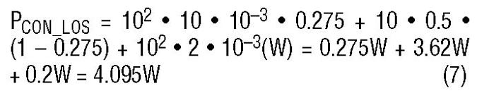
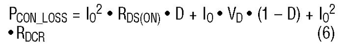 For example, a 12V input, 3.3V/10AMAX output buck supply can use following components: MOSFET RDS(ON) = 10mΩ, inductor RDCR = 2mΩ, diode forward voltage VD = 0.5V. Therefore, the conduction loss at full load is:
 Considering only conduction loss, the converter efficiency is:
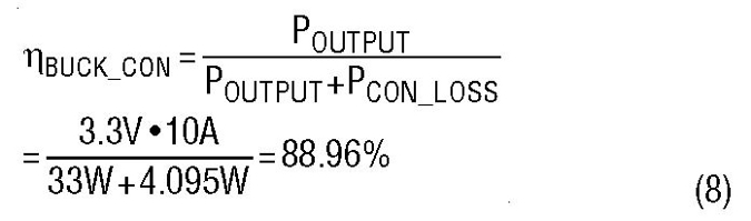 The above analysis shows that the freewheeling diode consumes 3.62W power loss, which is much higher than the conduction losses of the MOSFET Q1 and the inductor L. To further improve efficiency, diode D1 can be replaced with a MOSFET Q2, as shown in Figure 9. This converter is referred to as a synchronous buck converter. Q2’s gate requires signals complementary to the Q1 gate, i.e., Q2 is only on when Q1 is off. The conduction loss of the synchronous buck converter is:
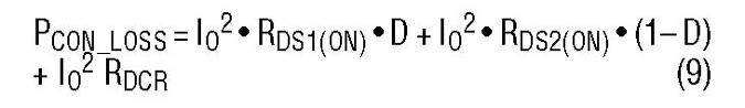 If a 10mΩ RDS(ON) MOSFET is used for Q2 as well, the conduction loss and efficiency of the synchronous buck converter are:
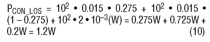
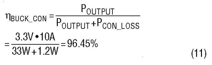 The above example shows that the synchronous buck is more efficient than a conventional buck converter, especially for low output voltage applications where the duty cycle is small and the conduction time of the diode D1 is long.
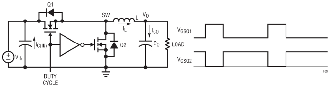 Figure 9. Synchronous Buck Converter and Its Transistor Gate Signals
- AC Switching Losses
In addition to the DC conduction losses, there are other AC/switching related power losses due to the non-ideal power components:
1. MOSFET switching losses. A real transistor requires time to be turned on or off. So there are voltage and current overlaps during the turn-on and turn-off transients, which generate AC switching losses. Figure 10 shows the typical switching waveforms of the MOSFET Q1 in the synchronous buck converter. The charging and discharging of the top FET Q1’s parasitic capacitor CGD with charge QGD determine most of the Q1 switching time and related losses.
In the synchronous buck, the bottom FET Q2 switching loss is small, because Q2 is always turned on after its body diode conducts and is turned off before its body diode conducts, while the voltage drop across the body diode is low. However, the body diode reverse recovery charge of Q2 can also increase the switching loss of the top FET Q1 and can generate switching voltage ringing and EMI noise. Equation (12) shows that the control FET Q1 switching loss is proportional to the converter switching frequency fS. The accurate calculation of the energy losses EON and EOFF for Q1 is not simple but can be found from MOSFET vendors’ application notes.
Figure 9. Synchronous Buck Converter and Its Transistor Gate Signals
- AC Switching Losses
In addition to the DC conduction losses, there are other AC/switching related power losses due to the non-ideal power components:
1. MOSFET switching losses. A real transistor requires time to be turned on or off. So there are voltage and current overlaps during the turn-on and turn-off transients, which generate AC switching losses. Figure 10 shows the typical switching waveforms of the MOSFET Q1 in the synchronous buck converter. The charging and discharging of the top FET Q1’s parasitic capacitor CGD with charge QGD determine most of the Q1 switching time and related losses.
In the synchronous buck, the bottom FET Q2 switching loss is small, because Q2 is always turned on after its body diode conducts and is turned off before its body diode conducts, while the voltage drop across the body diode is low. However, the body diode reverse recovery charge of Q2 can also increase the switching loss of the top FET Q1 and can generate switching voltage ringing and EMI noise. Equation (12) shows that the control FET Q1 switching loss is proportional to the converter switching frequency fS. The accurate calculation of the energy losses EON and EOFF for Q1 is not simple but can be found from MOSFET vendors’ application notes.
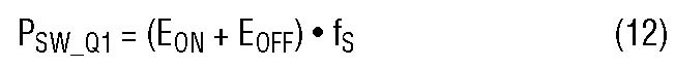
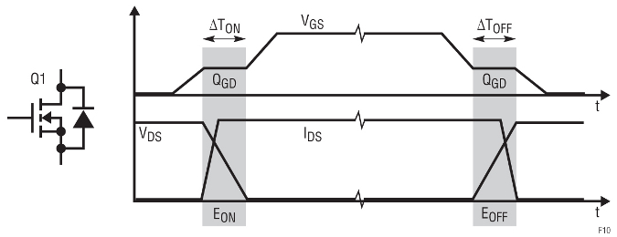 Figure 10. Typical Switching Waveform and Losses in the Top FET Q1 in the Buck Converter
2. Inductor core loss PSW_CORE. A real inductor also has AC loss that is a function of switching frequency. Inductor AC loss is primarily from the magnetic core loss. In a high frequency SMPS, the core material may be powdered iron or ferrite. In general, powdered iron cores saturate softly but have high core loss, while ferrite material saturates more sharply but has less core loss. Ferrites are ceramic ferromagnetic materials that have a crystalline structure consisting of mixtures of iron oxide with either manganese or zinc oxide. Core losses are due mainly to magnetic hysteresis loss. The core or inductor manufacturer usually provides the core loss data for power supply designers to estimate the AC inductor loss.
3. Other AC related losses. Other AC related losses include the gate driver loss PSW_GATE, which equals VDRV • QG • fS, and the dead time (when both top FET Q1 and bottom FET Q2 are off) body diode conduction loss, which is equal to (ΔTON + ΔTOFF) • VD(Q2) • fS.
In summary, the switching-related loss includes:
Figure 10. Typical Switching Waveform and Losses in the Top FET Q1 in the Buck Converter
2. Inductor core loss PSW_CORE. A real inductor also has AC loss that is a function of switching frequency. Inductor AC loss is primarily from the magnetic core loss. In a high frequency SMPS, the core material may be powdered iron or ferrite. In general, powdered iron cores saturate softly but have high core loss, while ferrite material saturates more sharply but has less core loss. Ferrites are ceramic ferromagnetic materials that have a crystalline structure consisting of mixtures of iron oxide with either manganese or zinc oxide. Core losses are due mainly to magnetic hysteresis loss. The core or inductor manufacturer usually provides the core loss data for power supply designers to estimate the AC inductor loss.
3. Other AC related losses. Other AC related losses include the gate driver loss PSW_GATE, which equals VDRV • QG • fS, and the dead time (when both top FET Q1 and bottom FET Q2 are off) body diode conduction loss, which is equal to (ΔTON + ΔTOFF) • VD(Q2) • fS.
In summary, the switching-related loss includes:
 [chapter-index=Index Head link-to=33057,33082]Application Note: P281[/chapter-index]The calculation of switching related losses is usually not easy. The switching related losses are proportional to switching frequency fS. In the 12VIN, 3.3VO/10AMAX synchronous buck converter, the AC loss causes about 2% to 5% efficiency loss with 200kHz – 500kHz switching frequency. So the overall efficiency is about 93% at full load, much better than that of an LR or LDO supply. The heat or size reduction can be close to 10x.
Where TON is the on-time interval within the switching period TS. If the ratio of TON/TS is defined as duty cycle D, the output voltage VO is:
When the filter inductor L and output capacitor CO values are sufficiently high, the output voltage VO is a DC voltage with only mV ripple. In this case, for a 12V input buck supply, conceptually, a 27.5% duty cycle provides a 3.3V output voltage.
Other than the above averaging approach, there is another way to derive the duty cycle equation. The ideal inductor cannot have DC voltage in steady state. So it must maintain inductor volt-second balance within a switching period. According to the inductor voltage waveform in Figure 8, volt-second balance requires:Zoom image: Figure 8. Buck Converter Operating Modes and Typical Waveforms / © Linear Technology
 Equation (5) is the same as equation (3). The same volt-second balance approach can be used for other DC/DC topologies to derive the duty cycle vs. VIN and VO equations.
Power Losses in a Buck Converter
- DC Conduction Losses
With ideal components (zero voltage drop in the ON state and zero switching loss), an ideal buck converter is 100% efficient. In reality, power dissipation is always associated with every power component. There are two types of losses in an SMPS: DC conduction losses and AC switching losses.
The conduction losses of a buck converter primarily result from voltage drops across transistor Q1, diode D1 and inductor L when they conduct current. To simplify the discussion, the AC ripple of inductor current is neglected in the following conduction loss calculation. If a MOSFET is used as the power transistor, the conduction loss of the MOSFET equals IO2 • RDS(ON) • D, where RDS(ON) is the on-resistance of MOSFET Q1. The conduction power loss of the diode equals IO • VD • (1 – D), where VD is the forward voltage drop of the diode D1. The conduction loss of the inductor equals IO2 • RDCR, where RDCR is the copper resistance of the inductor winding. Therefore, the conduction loss of the buck converter is approximately:
For example, a 12V input, 3.3V/10AMAX output buck supply can use following components: MOSFET RDS(ON) = 10mΩ, inductor RDCR = 2mΩ, diode forward voltage VD = 0.5V. Therefore, the conduction loss at full load is:
Considering only conduction loss, the converter efficiency is:
The above analysis shows that the freewheeling diode consumes 3.62W power loss, which is much higher than the conduction losses of the MOSFET Q1 and the inductor L. To further improve efficiency, diode D1 can be replaced with a MOSFET Q2, as shown in Figure 9. This converter is referred to as a synchronous buck converter. Q2’s gate requires signals complementary to the Q1 gate, i.e., Q2 is only on when Q1 is off. The conduction loss of the synchronous buck converter is:
If a 10mΩ RDS(ON) MOSFET is used for Q2 as well, the conduction loss and efficiency of the synchronous buck converter are:
The above example shows that the synchronous buck is more efficient than a conventional buck converter, especially for low output voltage applications where the duty cycle is small and the conduction time of the diode D1 is long.
Figure 9. Synchronous Buck Converter and Its Transistor Gate Signals
- AC Switching Losses
In addition to the DC conduction losses, there are other AC/switching related power losses due to the non-ideal power components:
1. MOSFET switching losses. A real transistor requires time to be turned on or off. So there are voltage and current overlaps during the turn-on and turn-off transients, which generate AC switching losses. Figure 10 shows the typical switching waveforms of the MOSFET Q1 in the synchronous buck converter. The charging and discharging of the top FET Q1’s parasitic capacitor CGD with charge QGD determine most of the Q1 switching time and related losses.
In the synchronous buck, the bottom FET Q2 switching loss is small, because Q2 is always turned on after its body diode conducts and is turned off before its body diode conducts, while the voltage drop across the body diode is low. However, the body diode reverse recovery charge of Q2 can also increase the switching loss of the top FET Q1 and can generate switching voltage ringing and EMI noise. Equation (12) shows that the control FET Q1 switching loss is proportional to the converter switching frequency fS. The accurate calculation of the energy losses EON and EOFF for Q1 is not simple but can be found from MOSFET vendors’ application notes.
Figure 10. Typical Switching Waveform and Losses in the Top FET Q1 in the Buck Converter
2. Inductor core loss PSW_CORE. A real inductor also has AC loss that is a function of switching frequency. Inductor AC loss is primarily from the magnetic core loss. In a high frequency SMPS, the core material may be powdered iron or ferrite. In general, powdered iron cores saturate softly but have high core loss, while ferrite material saturates more sharply but has less core loss. Ferrites are ceramic ferromagnetic materials that have a crystalline structure consisting of mixtures of iron oxide with either manganese or zinc oxide. Core losses are due mainly to magnetic hysteresis loss. The core or inductor manufacturer usually provides the core loss data for power supply designers to estimate the AC inductor loss.
3. Other AC related losses. Other AC related losses include the gate driver loss PSW_GATE, which equals VDRV • QG • fS, and the dead time (when both top FET Q1 and bottom FET Q2 are off) body diode conduction loss, which is equal to (ΔTON + ΔTOFF) • VD(Q2) • fS.
In summary, the switching-related loss includes:
[chapter-index=Index Head link-to=33057,33082]Application Note: P281[/chapter-index]The calculation of switching related losses is usually not easy. The switching related losses are proportional to switching frequency fS. In the 12VIN, 3.3VO/10AMAX synchronous buck converter, the AC loss causes about 2% to 5% efficiency loss with 200kHz – 500kHz switching frequency. So the overall efficiency is about 93% at full load, much better than that of an LR or LDO supply. The heat or size reduction can be close to 10x.
Equation (5) is the same as equation (3). The same volt-second balance approach can be used for other DC/DC topologies to derive the duty cycle vs. VIN and VO equations.
Power Losses in a Buck Converter
- DC Conduction Losses
With ideal components (zero voltage drop in the ON state and zero switching loss), an ideal buck converter is 100% efficient. In reality, power dissipation is always associated with every power component. There are two types of losses in an SMPS: DC conduction losses and AC switching losses.
The conduction losses of a buck converter primarily result from voltage drops across transistor Q1, diode D1 and inductor L when they conduct current. To simplify the discussion, the AC ripple of inductor current is neglected in the following conduction loss calculation. If a MOSFET is used as the power transistor, the conduction loss of the MOSFET equals IO2 • RDS(ON) • D, where RDS(ON) is the on-resistance of MOSFET Q1. The conduction power loss of the diode equals IO • VD • (1 – D), where VD is the forward voltage drop of the diode D1. The conduction loss of the inductor equals IO2 • RDCR, where RDCR is the copper resistance of the inductor winding. Therefore, the conduction loss of the buck converter is approximately:
For example, a 12V input, 3.3V/10AMAX output buck supply can use following components: MOSFET RDS(ON) = 10mΩ, inductor RDCR = 2mΩ, diode forward voltage VD = 0.5V. Therefore, the conduction loss at full load is:
Considering only conduction loss, the converter efficiency is:
The above analysis shows that the freewheeling diode consumes 3.62W power loss, which is much higher than the conduction losses of the MOSFET Q1 and the inductor L. To further improve efficiency, diode D1 can be replaced with a MOSFET Q2, as shown in Figure 9. This converter is referred to as a synchronous buck converter. Q2’s gate requires signals complementary to the Q1 gate, i.e., Q2 is only on when Q1 is off. The conduction loss of the synchronous buck converter is:
If a 10mΩ RDS(ON) MOSFET is used for Q2 as well, the conduction loss and efficiency of the synchronous buck converter are:
The above example shows that the synchronous buck is more efficient than a conventional buck converter, especially for low output voltage applications where the duty cycle is small and the conduction time of the diode D1 is long.
Figure 9. Synchronous Buck Converter and Its Transistor Gate Signals
- AC Switching Losses
In addition to the DC conduction losses, there are other AC/switching related power losses due to the non-ideal power components:
1. MOSFET switching losses. A real transistor requires time to be turned on or off. So there are voltage and current overlaps during the turn-on and turn-off transients, which generate AC switching losses. Figure 10 shows the typical switching waveforms of the MOSFET Q1 in the synchronous buck converter. The charging and discharging of the top FET Q1’s parasitic capacitor CGD with charge QGD determine most of the Q1 switching time and related losses.
In the synchronous buck, the bottom FET Q2 switching loss is small, because Q2 is always turned on after its body diode conducts and is turned off before its body diode conducts, while the voltage drop across the body diode is low. However, the body diode reverse recovery charge of Q2 can also increase the switching loss of the top FET Q1 and can generate switching voltage ringing and EMI noise. Equation (12) shows that the control FET Q1 switching loss is proportional to the converter switching frequency fS. The accurate calculation of the energy losses EON and EOFF for Q1 is not simple but can be found from MOSFET vendors’ application notes.
Figure 10. Typical Switching Waveform and Losses in the Top FET Q1 in the Buck Converter
2. Inductor core loss PSW_CORE. A real inductor also has AC loss that is a function of switching frequency. Inductor AC loss is primarily from the magnetic core loss. In a high frequency SMPS, the core material may be powdered iron or ferrite. In general, powdered iron cores saturate softly but have high core loss, while ferrite material saturates more sharply but has less core loss. Ferrites are ceramic ferromagnetic materials that have a crystalline structure consisting of mixtures of iron oxide with either manganese or zinc oxide. Core losses are due mainly to magnetic hysteresis loss. The core or inductor manufacturer usually provides the core loss data for power supply designers to estimate the AC inductor loss.
3. Other AC related losses. Other AC related losses include the gate driver loss PSW_GATE, which equals VDRV • QG • fS, and the dead time (when both top FET Q1 and bottom FET Q2 are off) body diode conduction loss, which is equal to (ΔTON + ΔTOFF) • VD(Q2) • fS.
In summary, the switching-related loss includes:
[chapter-index=Index Head link-to=33057,33082]Application Note: P281[/chapter-index]The calculation of switching related losses is usually not easy. The switching related losses are proportional to switching frequency fS. In the 12VIN, 3.3VO/10AMAX synchronous buck converter, the AC loss causes about 2% to 5% efficiency loss with 200kHz – 500kHz switching frequency. So the overall efficiency is about 93% at full load, much better than that of an LR or LDO supply. The heat or size reduction can be close to 10x.