© Linear Technology
Application Notes |
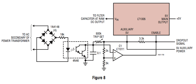 In some systems it is more convenient, or advantageous, to detect power outages by directly monitoring the AC line. Figure 8’s circuit does this by connecting an opto- isolator across the AC output of the power transformer.
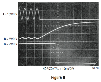
Normally, the AC line (Trace A, Figure 9) turns on the LED every 8ms (1/2 cycle of the line), causing the Darlington output transistor to reset the 0.01μF capacitor to VCE(SAT). When the line drops out (Trace B, Figure 9), the capacitor charges at a rate dependent upon the setting of the 20k potentiometer.
This ramping voltage is compared by C1 to a reference derived from the auxiliary output. When C1 goes low, the regulator output goes low (Trace C, Figure 9). This occurrence can be used as a logic signal to flag circuitry which is powered by the auxiliary output.
In some systems it is more convenient, or advantageous, to detect power outages by directly monitoring the AC line. Figure 8’s circuit does this by connecting an opto- isolator across the AC output of the power transformer.
Normally, the AC line (Trace A, Figure 9) turns on the LED every 8ms (1/2 cycle of the line), causing the Darlington output transistor to reset the 0.01μF capacitor to VCE(SAT). When the line drops out (Trace B, Figure 9), the capacitor charges at a rate dependent upon the setting of the 20k potentiometer.
This ramping voltage is compared by C1 to a reference derived from the auxiliary output. When C1 goes low, the regulator output goes low (Trace C, Figure 9). This occurrence can be used as a logic signal to flag circuitry which is powered by the auxiliary output.
Understanding and Applying the LT1005
LT1005 - developed a lifetime ago, but still in its prime today. This is an application note from Linear Technology (written by Jim Williams), which was published for the first time in August 1984.
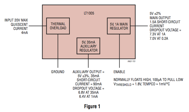
EDITOR'S NOTE_ Alle graphics © Linear Technology / All smaller graphics (as well as the top image have zoom function.The number of voltage regulators currently available makes the introduction of another regulator seem almost unnecessary. However, a new device, the LT1005, offers auxiliary functions which help solve problems often as- sociated with voltage regulation in circuits. The LT1005 (Figure 1) consists of a 5V, 1A1 regulator, which is controlled by a positive logic enable pin, and a 5V auxiliary regulator. The auxiliary regulator’s output is unaffected by the state of the main regulator.
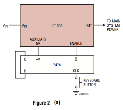
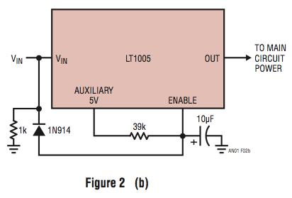
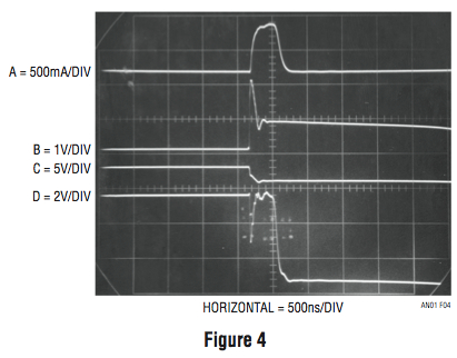
Thermal overload protection and current limiting round out the device. The enable pin is a high impedance input which floats in a high state. 10μA1 of current pulled from the pin will force it below its 1.6V turn-off threshold, shutting down the main output. Figure 2a shows a simple but useful application. Here, the regulator’s enable pin is controlled by the state of a toggling flip-flop which is triggered by a pushbutton on a computer keyboard. The auxiliary 5V output powers the flip-flop when the computer has been shut down. This arrangement allows the normal separate power switch to be eliminated. Although the enable pin interfaces directly to CMOS and TTL, its relatively high impedance allows it to implement a number of diverse functions. Figure 2b is a power-on delay circuit. Upon application of power, the output is held low until the capacitor charges beyond the 1.6V threshold of the enable pin. In this case, the time required is about 100ms. The diode-1k combina- tion drains the capacitor quickly when power is removed. Figure 2c shows a simple arrangement which will latch down the main regulator output if a short circuit occurs in the load. When power is applied to the regulator, the 5V auxiliary output comes up, transferring charge through the 10μF unit. This forces the enable pin high, allowing the main regulator to come up and power the load. If a load short occurs, the regulator goes into current limit and the main output falls to zero. This pulls the enable pin low, completing a positive feedback latch which disables the main regulator output. Under these conditions the output will remain at zero, even after the load short is removed. Also, the regulator will not have to dissipate power for the duration of the short circuit. The output may be reset by removing regulator input power or forcing the enable pin. Figure 3 illustrates a circuit which takes advantage of this operation to achieve a cost-effective solid-state equiva- lent of a circuit breaker. This circuit will turn off the main regulator’s output within 700ns of an overload. The trip current and breaker delay times are settable over a wide range. Under normal conditions the current through the 1Ω shunt is insufficient to bias Q1 into conduction. Q2 is also off and the regulator functions. When an overload occurs (Trace A, Figure 4 is the regulator’s output current), the potential across the 1Ω resistor rises, turning on Q1. A1’s collector drives Q2’s base (Trace B, Figure 4) via the 1k resistor and the 100pF speed-up capacitor. This turns on Q2, pulling the enable pin (Trace C, Figure 4) to ground and shutting down the regulator output (Trace D, Figure 4).-----
-----
-----
-----

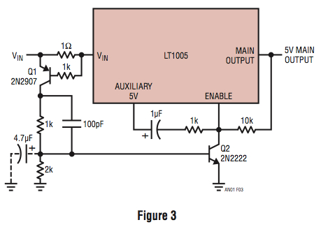
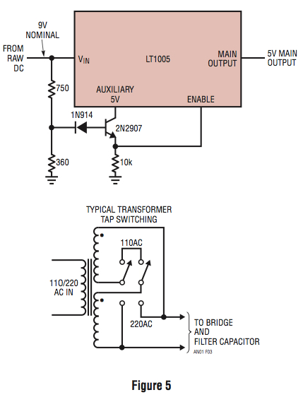
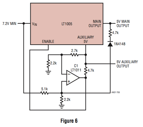
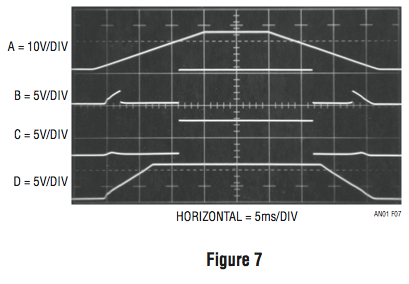
The 10k value from the main output to the enable pin latches the regulator down in a fashion similar to Figure 1 and the 4.7μF capacitor shown in dashed lines may be added (delete the 100pF unit) for applications where fast response is not desirable. The 1Ω value can be selected to accommodate any desired current trip point. Figure 5 shows another circuit which uses the enable pin to shut down the regulator under abnormal conditions. This configuration is useful in instruments or systems meant to be powered from 110VAC or 220VAC. Powering a regulator from a 220VAC primary when the secondary transformer tap switch is set for 110VAC forces excessive dissipation in the regulator, leading to thermal shutdown. The circuit shown prevents this by sensing the abnormally high input voltage and shutting down the regulator. Under normal operating conditions the input voltage is low enough to keep the transistor on, pulling the enable pin toward the auxiliary output and maintaining regulator output. If the circuit is inadvertently powered from 220VAC without moving the transformer tap switch, the regulator’s input voltage rises. This cuts off the transistor and the 10k re- sistor pulls the enable pin to ground, shutting down the regulator. The diode in the transistor’s base line prevents VBE zenering during the reverse bias condition which exists during the shutdown. For the values given, this circuit will function properly over ranges of 88VAC to 135VAC and 180VAC to 260VAC (110VAC to 220VAC ± 20%). Figure 6 shows the LT1005 in another circuit where opera- tion depends on input conditions. This circuit is useful in systems where it is necessary to bring up and power-down circuitry in a sequence. It is particularly applicable in situ- ations where it is desirable to transfer and store data into nonvolatile memory during power outages. It functions by taking advantage of the differing dropout voltages between the main and auxiliary outputs. When power is first applied, the LT1005 input (Trace A, Figure 7) starts to ramp up. The auxiliary output (Trace D, Figure 7) follows this ramping action and clamps at its 5V regulated output. During this interval, C1 monitors the difference between the regulator input and the 5V auxiliary output. The resis- tor ratios at its inputs are scaled so that the enable pin (Trace B, Figure 7) will be clamped until the regulator input is high enough to support main output regulation. (The small ramp segments visible at the enable pin are due to the comparator output’s failure to clamp under very low supply voltage conditions. The do not influence overall circuit operation). When this point is reached, the main output (Trace C, Figure 7) comes up quickly. Because the auxiliary output precedes the main output, it can be used to preset conditions in the circuitry being powered by the regulator. When power falls below the threshold point, C1 pulls the enable pin (Trace B, Figure 7) low, forcing the regulator’s main output to go off rapidly. The auxiliary output, however, maintains regulation after the main output has gone off. This allows the main output to be used as a logic signal to alert auxiliary-powered nonvolatile memory to store data. The amount of time the auxiliary output will maintain regulation on power-down may be controlled by regulator filter capacitor size. The diode-4.7k combination provides regenerative action to assure a clean turn-off for the main output.-----
-----
-----
 In some systems it is more convenient, or advantageous, to detect power outages by directly monitoring the AC line. Figure 8’s circuit does this by connecting an opto- isolator across the AC output of the power transformer.
Normally, the AC line (Trace A, Figure 9) turns on the LED every 8ms (1/2 cycle of the line), causing the Darlington output transistor to reset the 0.01μF capacitor to VCE(SAT). When the line drops out (Trace B, Figure 9), the capacitor charges at a rate dependent upon the setting of the 20k potentiometer.
This ramping voltage is compared by C1 to a reference derived from the auxiliary output. When C1 goes low, the regulator output goes low (Trace C, Figure 9). This occurrence can be used as a logic signal to flag circuitry which is powered by the auxiliary output.
In some systems it is more convenient, or advantageous, to detect power outages by directly monitoring the AC line. Figure 8’s circuit does this by connecting an opto- isolator across the AC output of the power transformer.
Normally, the AC line (Trace A, Figure 9) turns on the LED every 8ms (1/2 cycle of the line), causing the Darlington output transistor to reset the 0.01μF capacitor to VCE(SAT). When the line drops out (Trace B, Figure 9), the capacitor charges at a rate dependent upon the setting of the 20k potentiometer.
This ramping voltage is compared by C1 to a reference derived from the auxiliary output. When C1 goes low, the regulator output goes low (Trace C, Figure 9). This occurrence can be used as a logic signal to flag circuitry which is powered by the auxiliary output.
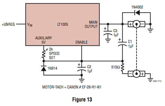
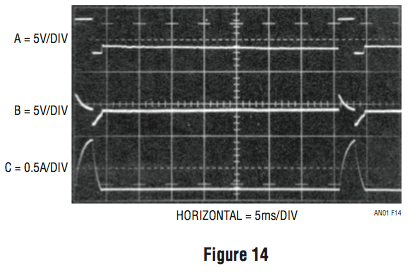
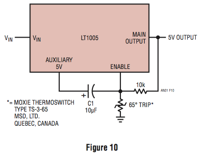
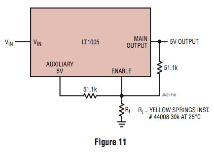
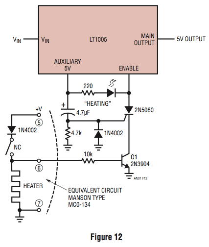
The “trip set” potentiometer and the value of the capacitor can be used to determine the number of missing line cycles required to shut down the regulator. When using this circuit it is important to recognize that the hold-up time of the raw supply must be taken into account to determine how long the auxiliary output will remain regulated. Figure 10 shows a latching circuit similar to Figure 2, ex- cept that a negative temperature coefficient (NTC) sharp transition thermistor runs from the enable pin to ground. This circuit will provide latching protection for circuitry under thermal overloads due to blocked vents or fan failures. The NTC device resistance decreases from 200k at 60°C to 10k at 65°C, cutting off the regulator. The thermistor is biased from the output, so latch-off occurs when the trip temperature is reached. C1 ensures starting. Unfortunately, the transition and hysteresis points of NTC devices are fixed and cannot be user varied. Figure 11 takes advantage of the relatively high impedance of the enable input to circumvent this problem. A standard thermistor (negative temperature coefficient) allows the trip point and hysteresis band to be set at any desired point. For the example shown, the regulator will shut down at 58°C ambient (8k thermistor resistance) and come back up at 42°C (15.2k thermistor resistance). Other characteristics are obtainable by shifting resistor and thermistor values. Figure 12 shows another thermally-related use of the regulator. The highest crystal oscillator stabilities are achieved by temperature-stabilizing the crystal. In frequency-measuring equipment and communications work it is often important that the crystal frequency be stabilized before the equipment is used. In this circuit, the LT1005 combines with a typical commercial crystal oven to prevent equipment use until oven temperature has stabilized. When power is applied, pin 6 of the crystal oven is high, biasing Q1. Simultaneously, the SCR gate is triggered by auxiliary-generated output current coming through the 4.7μF unit. This disables the main regulator output. When the oven reaches temperature, the thermo- switch opens, removing bias from Q1. This commutates the SCR and the regulator comes up, allowing its load to operate. The 4.7k resistor eliminates false SCR trigger- ing and the diode suppresses reverse gate current when regulator input power is removed. The latching action used in many of the preceding ap- plications is one form of feedback. Negative feedback to the enable pin can be used to make closed loop servos. Figure 13 shows a way to make a simple switched-mode motor speed controller with the LT1005. This circuit uses a tachometer to generate a feedback signal which is compared to a reference supplied by the auxiliary output. When power is applied, the tachometer output is zero and the regulator output (Trace A, Figure 14) comes on, forcing current (Trace C, Figure 14) into the motor.-----
-----
-----
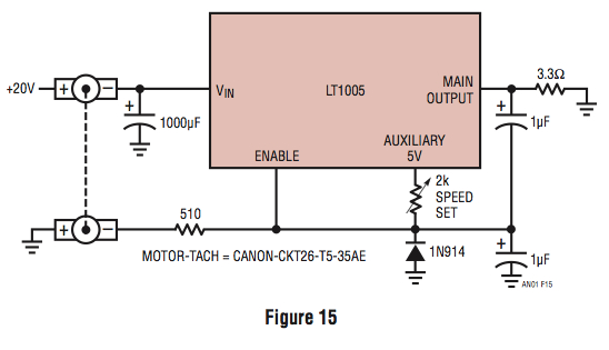
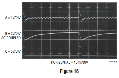
As motor rotation increases, the negative tachometer output pulls the enable pin (Trace B, Figure 14) toward ground. When the enable pin’s threshold voltage is reached, the regulator output goes down and the motor slows. C1 provides positive feedback, ensuring clean transitions. In this fashion, the motor’s speed is servo-controlled at a point determined by the 2k potentiometer setting. The regulator free-runs at whatever frequency and duty cycle are required to maintain the enable pin at its threshold. Loop bandwidth and stability are set by C2 and C3. The 1N914 diode prevents the negative output tachometer from pulling the enable pin below ground while the 1N4002 commutates the motor’s negative flyback pulse. The servo-controlled pulse mode excitation allows the motor to furnish excellent torque characteristics, even when operating at 5% of its full speed rating. For example, the small motor listed, with a shaft torque rating of 20 gram-cMs at 3300RPM, is almost unstoppable by the unaided human hand at 150RPM. The thermal and current limiting in the regulator prevents either the motor or the regulator from burning up in the event of a shaft overload. Figure 15 shows a way to run higher voltage motors. In this mode the motor is placed in the regulator input line and the output is terminated into a 3.3Ω load. The servo loop operates in a similar fashion to the one in Figure 13. In this case, however, a large capacitor is placed at the regulator to filter the transients generated by motor switching. When the tachometer output (Trace A, Figure 16) calls for power, the regulator comes on, allowing current to flow through the motor. This forces the regulator input toward ground (Trace B, Figure 16) for the duration of the on-time. The circuit’s advantage is that it allows higher voltage motors (up to 20V) to be controlled. In common with the previ- ous circuit, the regulator provides thermal and current overload protection for the motor. Its disadvantage is that for servo setpoints which require high motor power, the regulator’s DC input will go below dropout and the auxiliary output will fall, destabilizing the servo setpoint. Each of these circuits offers a simple, cost-effective, one package solution to speed control of small motors at the expense of efficiency. ----- Author: The Linear Technology AN01 was written by Jim Williams, who passed away on June 12, 2011. The picture shows him in his 'Analog-Workshop'; rather typical for him.-----
-----
-----