


© aydindurdu dreamstime.com
Application Notes |
Sum Current of both supplies is required to support the load
The LTC4370 is a 2-supply current sharing, diode-ORing controller that uses MOSFETs to form ideal diodes. In this way, the LTC4370 can actively balance the output currents of two supplies, even those with unequal output voltages.
This is a product release announcement by Linear Technology Corporation. The issuer is solely responsible for its content.
For two unequal voltage input supplies, the forward voltage of the higher voltage supply diode is servoed to balance the shared load current. The maximum allowable voltage drop is programmed by a resistor at the RANGE pin of the LTC4370.
Normally the LTC4370 is used to current share the outputs of two supplies, either of which is capable of providing the entire load current when its mate drops below the sharing voltage threshold set by the RANGE pin of the LTC4370 (see sidebar).
Nevertheless, the advantages of using the current sharing function can still be reaped in a non-redundant system, where the sum load current of two supplies is equal to, or in excess of that required by the load.
In normal operation, the LTC4370 allows the higher voltage supply to source all of the load current, however, in the case where the remaining supply is incapable of providing the full current, it is necessary to prevent such operation. This article describes a solution that disables the downstream load when this situation occurs.
Principal of Operation
In normal operation, the LTC4370 monitors the current of both supplies. Normally, with a perfect diode, the supply with the higher voltage would source all of the current to the load. The LTC4370 prevents this by linearly controlling the MOSFET of the higher voltage supply to provide current equal to that of the lower voltage supply. The maximum voltage difference allowed is determined by the resistor between the RANGE pin and ground.
When the input supply voltage difference rises beyond the programmed range, the LTC4370 disables the current sharing function. There are two alarm outputs, each monitoring the control voltage at the gate of each MOSFET. In normal operation, when either MOSFET is turned off (indicating a voltage difference beyond the programmed range) its associated FETON signal is set to a logic low.
In theory it seems that if these signals were passed through a logic AND function, they could be used to control the downstream load, disabling it when a MOSFET is turned off (indicating the loss of current sharing). These signals, however, both revert to logic low when zero current is passing through the MOSFET. In this situation, with the downstream load disabled and drawing no current, the system would remain in this state indefinitely.
The solution described here senses input voltage differences and disables the downstream load when a defined voltage difference between the supplies is detected. This voltage difference is programmed to be below the maximum voltage threshold of the LTC4370. If an out of balance condition is detected, the downstream power supply is disabled. To prevent an oscillatory condition, the circuit enters hiccup mode, where the supply is cycled on for 200ms every 3.2 seconds. The block diagram is shown in Figure 1.
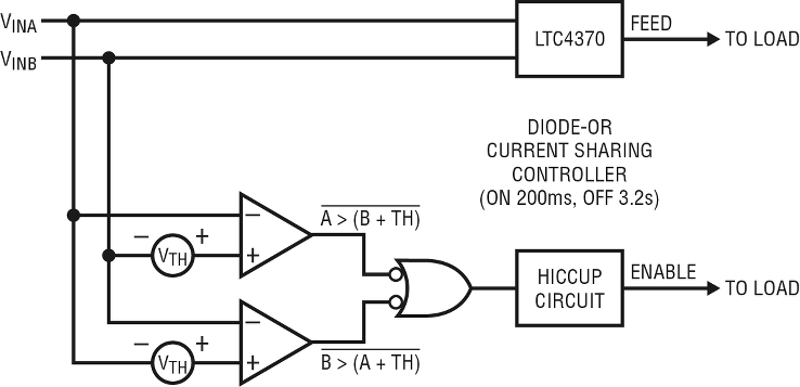 Figure 1. Block diagram of current summing circuitry
As shown in the block diagram, two comparators are used to sense when the absolute value of the difference between power supply inputs VINA and VINB is beyond that allowed for proper current sharing. When this happens, the output of the negative true OR gate is a logic high, enabling the hiccup circuit. Normally, the output of the hiccup circuit is a logic high, enabling the downstream load. When the out of range fault condition is detected, the hiccup circuit is activated, causing a logic low to disable the downstream load. The hiccup circuit monitors the voltage differential during the 200ms on period and is disabled when the fault condition is cleared.
Circuit Description
Figure 2 shows the complete solution. In Figure 2, U2 and U3 are LT1716 Over-The-Top voltage comparators used to detect voltage differences between VINA and VINB.
Threshold offset voltage to the comparators is provided by current sink transistors Q5 and Q6 in combination with R8 and R9. Current at the collectors of Q5 and Q6 is stabilized at 100µA by transistors Q1, Q2, Q3, and U6, an LT6650 voltage reference. In this case, R8 and R9 are set to 3.01k, resulting in an offset of 300mV. These resistor values can be changed to provide a different offset to match that of the LTC4370.
Figure 1. Block diagram of current summing circuitry
As shown in the block diagram, two comparators are used to sense when the absolute value of the difference between power supply inputs VINA and VINB is beyond that allowed for proper current sharing. When this happens, the output of the negative true OR gate is a logic high, enabling the hiccup circuit. Normally, the output of the hiccup circuit is a logic high, enabling the downstream load. When the out of range fault condition is detected, the hiccup circuit is activated, causing a logic low to disable the downstream load. The hiccup circuit monitors the voltage differential during the 200ms on period and is disabled when the fault condition is cleared.
Circuit Description
Figure 2 shows the complete solution. In Figure 2, U2 and U3 are LT1716 Over-The-Top voltage comparators used to detect voltage differences between VINA and VINB.
Threshold offset voltage to the comparators is provided by current sink transistors Q5 and Q6 in combination with R8 and R9. Current at the collectors of Q5 and Q6 is stabilized at 100µA by transistors Q1, Q2, Q3, and U6, an LT6650 voltage reference. In this case, R8 and R9 are set to 3.01k, resulting in an offset of 300mV. These resistor values can be changed to provide a different offset to match that of the LTC4370.
 Figure 2. Complete load sharing design
When either comparator U2 or U3 reaches the threshold determined by the offset, their output becomes logic low, enabling the hiccup circuit.
Figure 2. Complete load sharing design
When either comparator U2 or U3 reaches the threshold determined by the offset, their output becomes logic low, enabling the hiccup circuit.
Figure 1. Block diagram of current summing circuitry
As shown in the block diagram, two comparators are used to sense when the absolute value of the difference between power supply inputs VINA and VINB is beyond that allowed for proper current sharing. When this happens, the output of the negative true OR gate is a logic high, enabling the hiccup circuit. Normally, the output of the hiccup circuit is a logic high, enabling the downstream load. When the out of range fault condition is detected, the hiccup circuit is activated, causing a logic low to disable the downstream load. The hiccup circuit monitors the voltage differential during the 200ms on period and is disabled when the fault condition is cleared.
Circuit Description
Figure 2 shows the complete solution. In Figure 2, U2 and U3 are LT1716 Over-The-Top voltage comparators used to detect voltage differences between VINA and VINB.
Threshold offset voltage to the comparators is provided by current sink transistors Q5 and Q6 in combination with R8 and R9. Current at the collectors of Q5 and Q6 is stabilized at 100µA by transistors Q1, Q2, Q3, and U6, an LT6650 voltage reference. In this case, R8 and R9 are set to 3.01k, resulting in an offset of 300mV. These resistor values can be changed to provide a different offset to match that of the LTC4370.
Figure 2. Complete load sharing design
When either comparator U2 or U3 reaches the threshold determined by the offset, their output becomes logic low, enabling the hiccup circuit.
Load Summing Advantage A typical diode-OR system is a winner-take-all system where the highest voltage supply sources the entire load current. This one-supply-at-a-time scheme underutilizes the two supplies. The LTC4370’s current sharing diode-OR solution, on the other hand, reaps the benefits of sourcing and sharing current from both supplies:U4 is a 74HC132 quad CMOS NAND gate with hysteresis on each input. U5 is a 74HC163 4-bit programmable CMOS counter. The output of U4A is logic low when VINA and VINB is within the threshold determined by R8 and R9. When VINA and VINB is beyond this threshold, the corresponding comparator output becomes logic low, causing the output of U4A to become a logic high. A logic high output of U4A is inverted by U4B, producing a logic low at one input of NOR gate U4C. The resulting logic high output of U4C causes counter U5 to begin counting. The first count is zero, causing the TC (terminal count) pin to become logic low. This output remains low for the next 15 counts regardless of the input from U11B, due to the feedback from its output to the other input of NOR gate U4C. On count 16, the TC becomes high for a period of 200ms. During this period, the downstream load is enabled. If the comparators determine the voltage difference is within limits, the counter stops with the TC output remaining logic high, enabling the load. If the voltage difference is not within limits, the counter begins again, counting to 15 with the TC output a logic low. In this way, the load is enabled for 200ms every 3.2 seconds until the fault condition is cleared. The clock is provided by U4D, a hysteretic relaxation oscillator with a period of 200ms determined by R14 and C7. U1 is the LTC4370, which provides the current sharing function. The threshold is set to 300mV by R1. Operation of this device is described in the data sheet. Power for the additional circuitry is derived from VCC of the LTC4370. Conclusion The LTC4370 is designed primarily as a current sharing, diode-OR controller for two redundant supplies. With a few additional components, it can be easily used in a non-redundant supply environment as a robust load sharing controller, where both of the supplies are necessary to support the entire load. The solution described here provides that function. ----- Author: By Bob Smith, Mixed Signal Products, © Linear Technology Corp.
- Supply lifetimes are extended if each takes on half the load, spreading the supply heat and reducing thermal stresses on supply components.
- Because the lower voltage supply is always operational, there is no surprise when transitioning to a backup supply that may have already silently failed—a possibility in a simple diode-OR system.
- The recovery dynamics on supply failure are smoother and faster, since the supply changes are on the order of less and more, not off and on.
- A DC/DC converter formed by two supplies running at half capacity has better overall conversion efficiency than a single supply running near full capacity.