


© enruta dreamstime.com
Application Notes |
Basic concepts of linear regulator and switching mode power supplies
This article explains the basic concepts of linear regulators and switching mode power supplies (SMPS). It is aimed at system engineers who may not be very familiar with power supply designs and selection.
[chapter-index=Index Head link-to=33080,33082]Application Note: P281[/chapter-index]The basic operating principles of linear regulators and SMPS are explained and the advantages and disadvantages of each solution are discussed. The buck step-down converter is used as an example to further explain the design considerations of a switching regulator.
Introduction
Today’s designs require an increasing number of power rails and supply solutions in electronics systems, with loads ranging from a few mA for standby supplies to over 100A for ASIC voltage regulators. It is important to choose the appropriate solution for the targeted application and to meet specified performance requirements, such as high efficiency, tight printed circuit board (PCB) space, accurate output regulation, fast transient response, low solution cost, etc. Power management design is becoming a more frequent and challenging task for system designers, many of who may not have strong power backgrounds.
A power converter generates output voltage and current for the load from a given input power source. It needs to meet the load voltage or current regulation requirement during steady-state and transient conditions. It also must protect the load and system in case of a component failure. Depending on the specific application, a designer can choose either a linear regulator (LR) or a switching mode power supply (SMPS) solution. To make the best choice of a solution, it is essential for designers to be familiar with the merits, drawbacks and design concerns of each approach.
This article focuses on non-isolated power supply applications and provides an introduction to their operation and design basics.
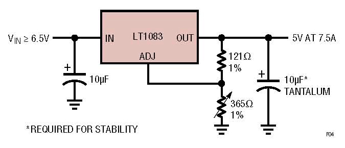 Figure 4. Integrated Linear Regulator Example: 7.5A Linear Regulator with Only Three Pins
Why Use Linear Regulators?
The linear regulator has been widely used by industry for a very long time. It was the basis for the power supply industry until switching mode power supplies became prevalent after the 1960s. Even today, linear regulators are still widely used in a wide range of applications. In addition to their simplicity of use, linear regulators have other performance advantages. Power management suppliers have developed many integrated linear regulators. A typical integrated linear regulator needs only VIN, VOUT, FB and optional GND pins.
Figure 4 shows a typical 3-pin linear regulator, the LT1083, which was developed more than 20 years ago by Linear Technology. It only needs an input capacitor, output capacitor and two feedback resistors to set the output voltage. Almost any electrical engineer can design a supply with these simple linear regulators.
One Drawback – A Linear Regulator Can Burn a Lot of Power
A major drawback of using linear regulators can be the excessive power dissipation of its series transistor Q1 operating in a linear mode. As explained previously, a linear regulator transistor is conceptually a variable resistor. Since all the load current must pass through the series transistor, its power dissipation is PLOSS = (VIN – VO) • IO. In this case, the efficiency of a linear regulator can be quickly estimated by:
Figure 4. Integrated Linear Regulator Example: 7.5A Linear Regulator with Only Three Pins
Why Use Linear Regulators?
The linear regulator has been widely used by industry for a very long time. It was the basis for the power supply industry until switching mode power supplies became prevalent after the 1960s. Even today, linear regulators are still widely used in a wide range of applications. In addition to their simplicity of use, linear regulators have other performance advantages. Power management suppliers have developed many integrated linear regulators. A typical integrated linear regulator needs only VIN, VOUT, FB and optional GND pins.
Figure 4 shows a typical 3-pin linear regulator, the LT1083, which was developed more than 20 years ago by Linear Technology. It only needs an input capacitor, output capacitor and two feedback resistors to set the output voltage. Almost any electrical engineer can design a supply with these simple linear regulators.
One Drawback – A Linear Regulator Can Burn a Lot of Power
A major drawback of using linear regulators can be the excessive power dissipation of its series transistor Q1 operating in a linear mode. As explained previously, a linear regulator transistor is conceptually a variable resistor. Since all the load current must pass through the series transistor, its power dissipation is PLOSS = (VIN – VO) • IO. In this case, the efficiency of a linear regulator can be quickly estimated by:
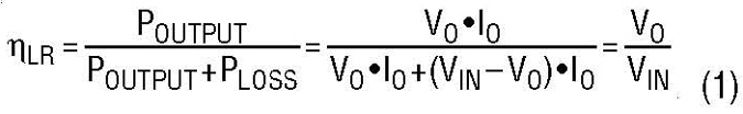 So in the Figure 1 example, when the input is 12V and output is 3.3V, the linear regulator efficiency is just 27.5%. In this case, 82.5% of the input power is just wasted and generates heat in the regulator. This means that the transistor must have the thermal capability to handle its power/heat dissipation at worst case at maximum VIN and full load. So the size of the linear regulator and its heat sink may be large, especially when VO is much less than VIN. Figure 5 shows that the maximum efficiency of the linear regulator is proportional to the VO/VIN ratio.
Linear Regulators How a Linear Regulator Works Let’s start with a simple example. In an embedded system, a 12V bus rail is available from the front-end power supply. On the system board, a 3.3V voltage is needed to power an operational amplifier (op amp). The simplest approach to generate the 3.3V is to use a resistor divider from the 12V bus, as shown in Figure 1. Does it work well? The answer is usually no. The op amp’s VCC pin current may vary under different operating conditions. If a fixed resistor divider is used, the IC VCC voltage varies with load. Besides, the 12V bus input may not be well regulated. There may be many other loads in the same system sharing the 12V rail. Because of the bus impedance, the 12V bus voltage varies with the bus loading conditions. As a result, a resistor divider cannot provide a regulated 3.3V to the op amp to ensure its proper operation. Therefore, a dedicated voltage regulation loop is needed. As shown in Figure 2, the feedback loop needs to adjust the top resistor R1 value to dynamically regulate the 3.3V on VCC. This kind of variable resistor can be implemented with a linear regulator, as shown in Figure 3. A linear regulator operates a bipolar or field effect power transistor (FET) in its linear mode. So the transistor works as a variable resistor in series with the output load. To establish the feedback loop, conceptually, an error amplifier senses the DC output voltage via a sampling resistor network RA and RB, and then compares the feedback voltage VFB with a reference voltage VREF. The error amplifier output voltage drives the base of the series power transistor via a current amplifier. When either the input VBUS voltage decreases or the load current increases, the VCC output voltage goes down. The feedback voltage VFB decreases as well. As a result, the feedback error amplifier and current amplifier generate more current into the base of the transistor Q1. This reduces the voltage drop VCE and hence brings back the VCC output voltage, so that VFB equals VREF. On the other hand, if the VCC output voltage goes up, in a similar way, the negative feedback circuit increases VCE to ensure the accurate regulation of the 3.3V output. In summary, any variation of VO is absorbed by the linear regulator transistor’s VCE voltage. So the output voltage VCC is always constant and well regulated.Figure 1. Resistor Divider Generates 3.3VDC from 12V Bus Input
Figure 2. Feedback Loop Adjusts Series Resistor R1 Value to Regulate 3.3V
Zoom image: Figure 3. A Linear Regulator Implements a Variable Resistor to Regulate Output Voltage Images: © Linear Technology
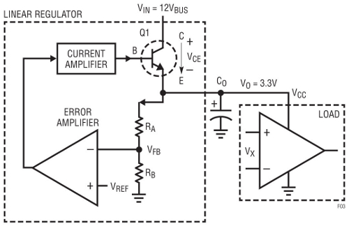 Figure 4. Integrated Linear Regulator Example: 7.5A Linear Regulator with Only Three Pins
Why Use Linear Regulators?
The linear regulator has been widely used by industry for a very long time. It was the basis for the power supply industry until switching mode power supplies became prevalent after the 1960s. Even today, linear regulators are still widely used in a wide range of applications. In addition to their simplicity of use, linear regulators have other performance advantages. Power management suppliers have developed many integrated linear regulators. A typical integrated linear regulator needs only VIN, VOUT, FB and optional GND pins.
Figure 4 shows a typical 3-pin linear regulator, the LT1083, which was developed more than 20 years ago by Linear Technology. It only needs an input capacitor, output capacitor and two feedback resistors to set the output voltage. Almost any electrical engineer can design a supply with these simple linear regulators.
One Drawback – A Linear Regulator Can Burn a Lot of Power
A major drawback of using linear regulators can be the excessive power dissipation of its series transistor Q1 operating in a linear mode. As explained previously, a linear regulator transistor is conceptually a variable resistor. Since all the load current must pass through the series transistor, its power dissipation is PLOSS = (VIN – VO) • IO. In this case, the efficiency of a linear regulator can be quickly estimated by:
So in the Figure 1 example, when the input is 12V and output is 3.3V, the linear regulator efficiency is just 27.5%. In this case, 82.5% of the input power is just wasted and generates heat in the regulator. This means that the transistor must have the thermal capability to handle its power/heat dissipation at worst case at maximum VIN and full load. So the size of the linear regulator and its heat sink may be large, especially when VO is much less than VIN. Figure 5 shows that the maximum efficiency of the linear regulator is proportional to the VO/VIN ratio.
Figure 4. Integrated Linear Regulator Example: 7.5A Linear Regulator with Only Three Pins
Why Use Linear Regulators?
The linear regulator has been widely used by industry for a very long time. It was the basis for the power supply industry until switching mode power supplies became prevalent after the 1960s. Even today, linear regulators are still widely used in a wide range of applications. In addition to their simplicity of use, linear regulators have other performance advantages. Power management suppliers have developed many integrated linear regulators. A typical integrated linear regulator needs only VIN, VOUT, FB and optional GND pins.
Figure 4 shows a typical 3-pin linear regulator, the LT1083, which was developed more than 20 years ago by Linear Technology. It only needs an input capacitor, output capacitor and two feedback resistors to set the output voltage. Almost any electrical engineer can design a supply with these simple linear regulators.
One Drawback – A Linear Regulator Can Burn a Lot of Power
A major drawback of using linear regulators can be the excessive power dissipation of its series transistor Q1 operating in a linear mode. As explained previously, a linear regulator transistor is conceptually a variable resistor. Since all the load current must pass through the series transistor, its power dissipation is PLOSS = (VIN – VO) • IO. In this case, the efficiency of a linear regulator can be quickly estimated by:
So in the Figure 1 example, when the input is 12V and output is 3.3V, the linear regulator efficiency is just 27.5%. In this case, 82.5% of the input power is just wasted and generates heat in the regulator. This means that the transistor must have the thermal capability to handle its power/heat dissipation at worst case at maximum VIN and full load. So the size of the linear regulator and its heat sink may be large, especially when VO is much less than VIN. Figure 5 shows that the maximum efficiency of the linear regulator is proportional to the VO/VIN ratio.
On the other hand, the linear regulator can be very efficient if VO is close to VIN. However, the linear regulator (LR) has another limitation, which is the minimum voltage difference between VIN and VO. The transistor in the LR must be operated in its linear mode. So it requires a certain minimum voltage drop across the collector to emitter of a bipolar transistor or drain to source of a FET. When VO is too close to VIN, the LR may be unable to regulate output voltage anymore. The linear regulators that can work with low headroom (VIN – VO) are called low dropout regulators (LDOs). It is also clear that a linear regulator or an LDO can only provide step-down DC/DC conversion. In applications that require VO voltage to be higher than VIN voltage, or need negative VO voltage from a positive VIN voltage, linear regulators obviously do not work. Linear Regulator with Current Sharing for High Power For applications that require more power, the regulator must be mounted separately on a heat sink to dissipate the heat. In all-surface-mount systems, this is not an option, so the limitation of power dissipation (1W for example) limits the output current. Unfortunately, it is not easy to directly parallel linear regulators to spread the generated heat. Replacing the voltage reference shown in Figure 3 with a precision current source, allows the linear regulator to be directly paralleled to spread the current load and thus spread dissipated heat among the ICs. This makes it possible to use linear regulators in high output current, all-surface-mount applications, where only a limited amount of heat can be dissipated in any single spot on a board.Figure 5. Maximum Linear Regulator Efficiency vs. VO/VIN Ratio
The LT3080 is the first adjustable linear regulator that can be used in parallel for higher current. As shown in Figure 6, it has a precision zero TC 10µA internal current source connected to the non-inverting input of the operational amplifier. With an external single voltage-setting resistor RSET, the linear regulator output voltage can be adjusted from 0V to (VIN – VDROPOUT). Figure 7 shows how easy it is to parallel LT3080s for current sharing. Simply tie the SET pins of the LT3080s together; the two regulators share the same reference voltage. Because the operational amplifiers are precisely trimmed, the offset voltage between the adjustment pin and the output is less than 2mV. In this case, only 10mΩ ballast resistance, which can be the sum of a small external resistor and PCB trace resistance, is needed to balance the load current with better than 80% equalized sharing. Need even more power? Even paralleling 5 to 10 devices is reasonable. Applications Where Linear Regulators Are Preferable There are many applications in which linear regulators or LDOs provide superior solutions to switching supplies, including: 1. Simple/low cost solutions. Linear regulator or LDO solutions are simple and easy to use, especially for low power applications with low output current where thermal stress is not critical. No external power inductor is required. 2. Low noise/low ripple applications. For noise-sensitive applications, such as communication and radio devices, minimizing the supply noise is very critical. Linear regulators have very low output voltage ripple because there are no elements switching on and off frequently and linear regulators can have very high bandwidth. So there is little EMI problem. Some special LDOs, such as Linear Technology’s LT1761 LDO family, have as low as 20μVRMS noise voltage on the output. It is almost impossible for an SMPS to achieve this low noise level. An SMPS usually has mV of output ripple even with very low ESR capacitors. 3. Fast transient applications. The linear regulator feedback loop is usually internal, so no external compensation is required. Typically, linear regulators have wider control loop bandwidth and faster transient response than that of SMPS. [chapter-index=Index Head link-to=33080,33082]Application Note: P281[/chapter-index]4. Low dropout applications. For applications where output voltage is close to the input voltage, LDOs may be more efficient than an SMPS. There are very low dropout LDOs (VLDO) such as Linear’s LTC1844, LT3020 and LTC3025 with from 20mV to 90mV dropout voltage and up to 150mA current. The minimum input voltage can be as low as 0.9V. Because there is no AC switching loss in an LR, the light load efficiency of an LR or an LDO is similar to its full load efficiency. An SMPS usually has lower light load efficiency because of its AC switching losses. In battery powered applications in which light load efficiency is also critical, an LDO can provide a better solution than an SMPS. In summary, designers use linear regulators or LDOs because they are simple, low noise, low cost, easy to use and provide fast transient response. If VO is close to VIN, an LDO may be more efficient than an SMPS.Figure 6. Single Resistor Setting LDO LT3080 with a Precision Current Source Reference
Figure 7. Paralleling of Two LT3080 Linear Regulators for Higher Output Current