
© juan-jose-tugores-gaspar-dreamstime.com
Application Notes |
Banishing those accursed spikes
Linear regulators are commonly employed to post-regulate switching regulator outputs. Benefits include improved stability, accuracy, transient response and lowered output impedance.
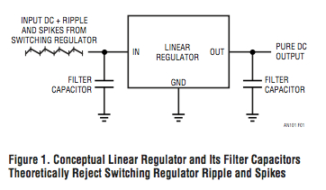
EDITOR'S NOTE_ All images have zoom function. © Linear Technology[chapter-index=Linear Technology AN101 link-to=24929, 24930, 24931, 24932, 24933]Please use the links below to navigate to the other parts of this application note.[/chapter-index]Ideally, these performance gains would be accompanied by markedly reduced switching regulator generated ripple and spikes. In practice, all linear regulators encounter some difficulty with ripple and spikes, particularly as frequency rises. This effect is magnified at small regulator VIN to VOUT differential voltages; unfortunate, because such small differentials are desirable to maintain efficiency. Figure 1 shows a conceptual linear regulator and associated components driven from a switching regulator output. The input filter capacitor is intended to smooth the ripple and spikes before they reach the regulator. The output capacitor maintains low output impedance at higher frequencies, improves load transient response and supplies frequency compensation for some regulators. Ancillary purposes include noise reduction and minimization of residual inputderived artifacts appearing at the regulators output. It is this last category–residual input-derived artifacts–that is of concern. These high frequency components, even though small amplitude, can cause problems in noise-sensitive video, communication and other types of circuitry. Large numbers of capacitors and aspirin have been expended in attempts to eliminate these undesired signals and their resultant effects. Although they are stubborn and sometimes seemingly immune to any treatment, understanding their origin and nature is the key to containing them.
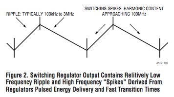
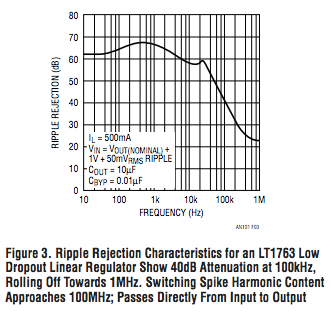
Switching Regulator AC Output Content Figure 2 details switching regulator dynamic (AC) output content. It consists of relatively low frequency ripple at the switching regulator’s clock frequency, typically 100kHz to 3MHz, and very high frequency content “spikes” associated with power switch transition times. The switching regulator’s pulsed energy delivery creates the ripple. Filter capacitors smooth the output, but not completely. The spikes, which often have harmonic content approaching 100MHz, result from high energy, rapidly switching power elements within the switching regulator. The filter capacitor is intended to reduce these spikes but in practice cannot entirely eliminate them. Slowing the regulator’s repetition rate and transition times can greatly reduce ripple and spike amplitude, but magnetics size increases and efficiency falls1. The same rapid clocking and fast switching that allows small magnetics size and high efficiency results in high frequency ripple and spikes presented to the linear regulator. Ripple and Spike Rejection The regulator is better at rejecting the ripple than the very wideband spikes. Figure 3 shows rejection performance for an LT1763 low dropout linear regulator. There is 40db attenuation at 100KHz, rolling off to about 25db at 1MHz. The much more wideband spikes pass directly through the regulator. The output filter capacitor, intended to absorb the spikes, also has high frequency performance limitations. The regulator and fi lter capacitors imperfect response, due to high frequency parasitics, reveals Figure 1 to be overly simplistic. Figure 4 restates Figure 1 and includes the parasitic terms as well as some new components. The figure considers the regulation path with emphasis on high frequency parasitics. It is important to identify these parasitic terms because they allow ripple and spikes to propagate into the nominally regulated output. Additionally, understanding the parasitic elements permits a measurement strategy, facilitating reduction of high frequency output content. The regulator includes high frequency parasitic paths, primarily capacitive, across its pass transistor and into its reference and regulation amplifier. These terms combine with finite regulator gain-bandwidth to limit high frequency rejection. The input and output filter capacitors include parasitic inductance and resistance, degrading their effectiveness as frequency rises.-----
-----
-----
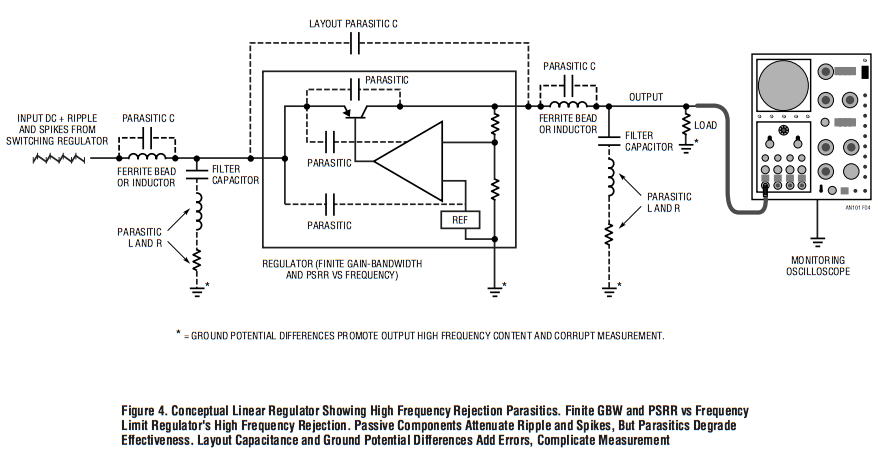
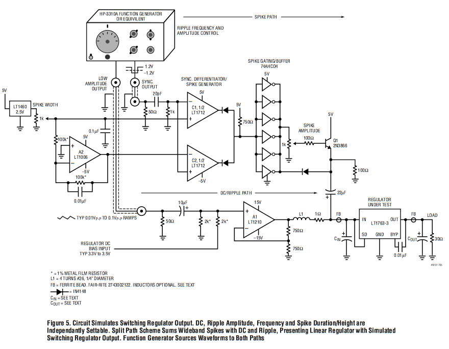
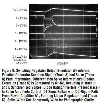
Stray layout capacitance provides additional unwanted feedthrough paths. Ground potential differences, promoted by ground path resistance and inductance, add additional error and also complicate measurement. Some new components, not normally associated with linear regulators, also appear. These additions include ferrite beads or inductors in the regulator input and output lines. These components have their own high frequency parasitic paths but can considerably improve overall regulator high frequency rejection and will be addressed in following text. Ripple/Spike Simulator Gaining understanding of the problem requires observing regulator response to ripple and spikes under a variety of conditions. It is desirable to be able to independently vary ripple and spike parameters, including frequency, harmonic content, amplitude, duration and DC level. This is a very versatile capability, permitting real time optimization and sensitivity analysis to various circuit variations. Although there is no substitute for observing linear regulator performance under actual switching regulator driven conditions, a hardware simulator makes surprises less likely. Figure 5 provides this capability. It simulates a switching regulator’s output with independantly settable DC, ripple and spike parameters. A commercially available function generator combines with two parallel signal paths to form the circuit. DC and ripple are transmitted on a relatively slow path while wideband spike information is processed via a fast path. The two paths are combined at the linear regulator input. The function generator’s settable ramp output (trace A, Figure 6) feeds the DC/ripple path made up of power amplifier A1 and associated components. A1 receives the ramp input and DC bias information and drives the regulator under test. L1 and the 1Ω resistor allow A1 to drive the regulator at ripple frequencies without instability. The wideband spike path is sourced from the function generator’s pulsed “sync” output (trace B). This output’s edges are differentiated (trace C) and fed to bipolar comparator C1-C2. The comparator outputs (traces D and E) are spikes synchronized to the ramps infl ection points. Spike width is controlled by complementary DC threshold potentials applied to C1 and C2 with the 1k potentiometer and A2. Diode gating and the paralleled logic inverters present trace F to the spike amplitude control. Follower Q1 sums the spikes with A1’s DC/ripple path, forming the linear regulator’s input (trace G).-----
-----
-----
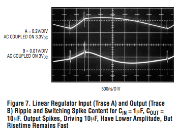
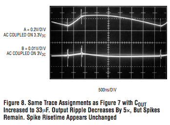
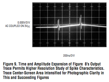
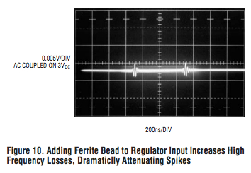
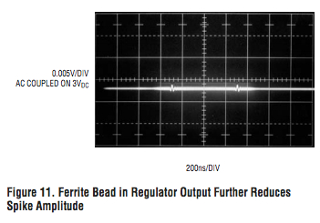
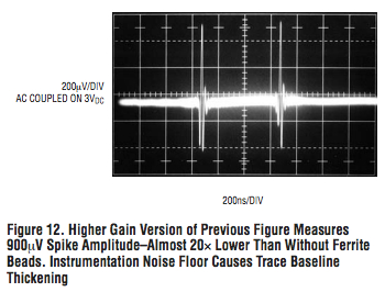
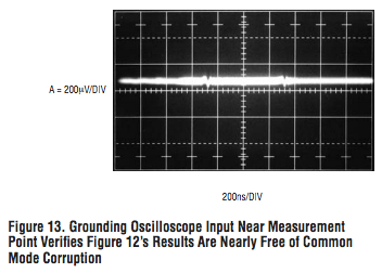
Linear Regulator High Frequency Rejection Evaluation/Optimization The circuit described above facilitates evaluation and optimization of linear regulator high frequency rejection. The following photographs show results for one typical set of conditions, but DC bias, ripple and spike characteristics may be varied to suit desired test parameters. Figure 7 shows Figure 5’s LT1763 3V regulator response to a 3.3V DC input with trace A’s ripple/spike contents, CIN = 1μF and COUT = 10μF. Regulator output (trace B) shows ripple attenuated by a factor of ≈ 20. Output spikes see somewhat less reduction and their harmonic content remains high. The regulator offers no rejection at the spike rise time. The capacitors must do the job. Unfortunately, the capacitors are limited by inherent high frequency loss terms from completely filtering the wideband spikes; trace B’s remaining spike shows no risetime reduction. Increasing capacitor value has no benefit at these rise times. Figure 8 (same trace assignments as Figure 7) taken with COUT = 33μF, shows 5× ripple reduction but little spike amplitude attenuation. Figure 9’s time and amplitude expansion of Figure 8’s trace B permits high resolution study of spike characteristics, allowing the following evaluation and optimization. Figure 10 shows dramatic results when a ferrite bead immediately precedes CIN2. Spike amplitude drops about 5×. The bead presents loss at high frequency, severely limiting spike passage3. DC and low frequency pass unattenuated to the regulator. Placing a second ferrite bead at the regulator output before COUT produces Figure 11’s trace. The bead’s high frequency loss characteristic further reduces spike amplitude below 1mV without introducing DC resistance into the regulator’s output path4. Figure 12, a higher gain version of the previous fi gure, measures 900µV spike amplitude – almost 20× lower than without the ferrite beads. The measurement is completed by verifying that indicated results are not corrupted by common mode components or ground loops. This is done by grounding the oscilloscope input near the measurement point. Ideally, no signal should appear. Figure 13 shows this to be nearly so, indicating that Figure 12’s display is realistic5.-----
-----
-----
-----