


© tilltibet dreamstime.com
Analysis |
Samsung invests big to maintain leadership
Samsung recently announced plans to build a new, cutting-edge wafer fab—a $14.7 billion investment for the company that will be located in Pyeongtaek, a city south of Seoul.
The new fab, slated to begin production in 2H17, will add to Samsung’s current impressive compilation of wafer fabs (Figure 1) as it seeks to maintain its leading position in memory IC sales and expand its system leadership beyond smartphones, Smart TVs, and tablets. Investing large is not new to Samsung—it has allocated at least $10 billion per year on semiconductor capital expenditures since 2010 (Figure 2), and has accounted for 17-21% of total industry capital expenditures each year since then.
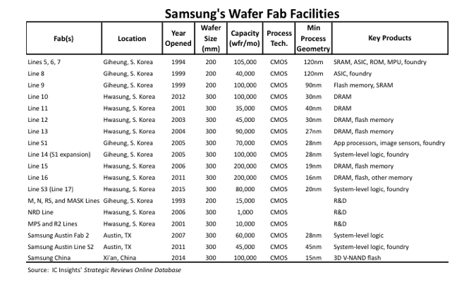 Figure 1
Samsung did not identify specifically which chips will be manufactured at the new fab, but given its current market strength in smartphones, Smart TVs, and tablet PCs, it is reasonable to believe it will set up operations to produce logic and memory devices—DRAM, flash memory (including perhaps its new 3D V-NAND flash memory), and application processors—that are the brains and storage in these systems. In addition, the growing adoption rate for solid-state drives (SSDs) and the potential growth and development of the Internet of Things are emerging market segments that Samsung believes will fuel demand for its memory and logic chips in the coming years.
Samsung is also likely to give strong consideration to foundry operations at the new fab. It is well known that Samsung lost the Apple A8 processor business to TSMC. Yet despite losing a $2 billion foundry customer, foundry work remains an important segment for Samsung, and the company is committed to growing this business. Its leading-edge manufacturing capabilities make it an attractive option for several fabless and fab-lite logic IC companies.
Figure 1
Samsung did not identify specifically which chips will be manufactured at the new fab, but given its current market strength in smartphones, Smart TVs, and tablet PCs, it is reasonable to believe it will set up operations to produce logic and memory devices—DRAM, flash memory (including perhaps its new 3D V-NAND flash memory), and application processors—that are the brains and storage in these systems. In addition, the growing adoption rate for solid-state drives (SSDs) and the potential growth and development of the Internet of Things are emerging market segments that Samsung believes will fuel demand for its memory and logic chips in the coming years.
Samsung is also likely to give strong consideration to foundry operations at the new fab. It is well known that Samsung lost the Apple A8 processor business to TSMC. Yet despite losing a $2 billion foundry customer, foundry work remains an important segment for Samsung, and the company is committed to growing this business. Its leading-edge manufacturing capabilities make it an attractive option for several fabless and fab-lite logic IC companies.
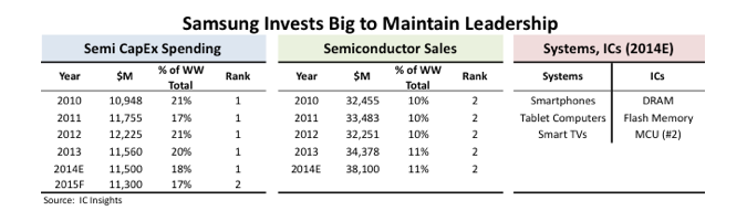 Figure 2 / © IC Insights
The decision by Samsung to build a new, large wafer fab comes at a time when the semiconductor industry is facing several major hurdles. These include the transition to 450mm wafers and EUV lithography, the physical limitations of manufacturing existing DRAM and flash memory designs using sub 10nm process technology, and the possible transition to alternative memories. On one hand, the company faces some big decisions on which way to proceed, but investing now assures Samsung will be at the leading edge in manufacturing and delivering advanced devices at a competitive cost.
Figure 2 / © IC Insights
The decision by Samsung to build a new, large wafer fab comes at a time when the semiconductor industry is facing several major hurdles. These include the transition to 450mm wafers and EUV lithography, the physical limitations of manufacturing existing DRAM and flash memory designs using sub 10nm process technology, and the possible transition to alternative memories. On one hand, the company faces some big decisions on which way to proceed, but investing now assures Samsung will be at the leading edge in manufacturing and delivering advanced devices at a competitive cost.
Figure 1
Samsung did not identify specifically which chips will be manufactured at the new fab, but given its current market strength in smartphones, Smart TVs, and tablet PCs, it is reasonable to believe it will set up operations to produce logic and memory devices—DRAM, flash memory (including perhaps its new 3D V-NAND flash memory), and application processors—that are the brains and storage in these systems. In addition, the growing adoption rate for solid-state drives (SSDs) and the potential growth and development of the Internet of Things are emerging market segments that Samsung believes will fuel demand for its memory and logic chips in the coming years.
Samsung is also likely to give strong consideration to foundry operations at the new fab. It is well known that Samsung lost the Apple A8 processor business to TSMC. Yet despite losing a $2 billion foundry customer, foundry work remains an important segment for Samsung, and the company is committed to growing this business. Its leading-edge manufacturing capabilities make it an attractive option for several fabless and fab-lite logic IC companies.
Figure 2 / © IC Insights
The decision by Samsung to build a new, large wafer fab comes at a time when the semiconductor industry is facing several major hurdles. These include the transition to 450mm wafers and EUV lithography, the physical limitations of manufacturing existing DRAM and flash memory designs using sub 10nm process technology, and the possible transition to alternative memories. On one hand, the company faces some big decisions on which way to proceed, but investing now assures Samsung will be at the leading edge in manufacturing and delivering advanced devices at a competitive cost.