


© Analog Devices Inc.
Application Notes |
Pocket-Size white noise generator for quickly testing circuit signal response
Question: Can you produce a frequency spectrum for all frequencies at the same time?
Answer: Noise in electrical circuits is typically the enemy, and any self-respecting circuit should output as little noise as possible. Nevertheless, there are cases where a well-characterized source of noise with no other signal is entirely the desired output.
Circuit characterization is such a case. The outputs of many circuits can be characterized by sweeping the input signal across a range of frequencies and observing the response of the design. Input sweeps can be composed of discrete input frequencies or a swept sine. Extremely low frequency sine waves (below 10 Hz) are difficult to produce cleanly. A processor, DAC, and some complex, precise filtering can produce relatively clean sine waves, but for each frequency step, the system must settle, making slow work of sequential full sweeps featuring many frequencies. Testing fewer discrete frequencies can be faster, but increases the risk of skipping over critical frequencies where high Q phenomena reside.
A white noise generator is simpler and faster than a swept sine wave because it effectively produces all frequencies at the same time with the same amplitude. Imposing white noise at the input of a device under test (DUT) can quickly produce an overview of the frequency response over an entire frequency range. In this case, there is no need for expensive or complex swept sine wave generators. Simply connect the DUT output to a spectrum analyzer and watch. Using more averaging and longer acquisition times produces a more accurate output response across the frequency range of interest.
The expected response of the DUT to white noise is frequency-shaped noise. Using white noise in this fashion can quickly expose unexpected behavior such as weird frequency spurs, strange harmonics, and undesirable frequency response artifacts.
Furthermore, a white noise generator allows a careful engineer to test a tester. Lab equipment that measures frequency response should produce a flat noise profile when measuring a known flat white noise generator.
On the practical side, a white noise generator is easy to use, small enough for compact lab setups, portable for field measurements, and inexpensive. Quality signal generators with myriad settings are attractively versatile. However, versatility can hamper quick frequency response measurements. A well-designed white noise generator requires no controls, yet produces a fully predictable output.
Noisy Discussion
Resistor thermal noise, sometimes called Johnson noise or Nyquist noise, arises from thermal agitation of charge carriers inside a resistor. This noise is approximately white, with nearly Gaussian distribution. In electrical terms, the noise voltage density is given by
VNOISE = √4kBTR
where kB is the Boltzmann’s constant, T is the temperature in Kelvin, and R is the resistance. Noise voltage arises from the random movement of charges flowing through the basic resistance, a sort of R × INOISE. Table 1 shows examples at 20°C.
Table 1. Noise Voltage Density of Various Resistors
A 10 MΩ resistor, then, represents a 402 nV⁄√Hz wideband voltage noise source in series with the nominal resistance. A gained up resistor-derived noise source is fairly stable as a lab test noise source, as R and T variations affect noise only by square root. For instance, a change of 6°C from 20°C is a change of 293 kΩ to 299 kΩ. Because noise density is directly proportional to the square root of temperature, a change of 6°C temperature leads to a relatively small 1% noise density change. Similarly, with resistance, a 2% resistance change leads to a 1% noise density change.
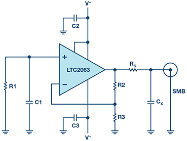 Figure 1. Full schematic of white noise generator. Low drift micropower LTC2063 amplifies the Johnson noise of R1.
Consider Figure 1: a 10 MΩ resistor R1 generates white, Gaussian noise at the positive terminal of an op amp. Resistors R2 and R3 gain the noise voltage to the output. Capacitor C1 filters out chopper amplifier charge glitches. Output is a 10 µV/√Hz white noise signal.
Gain (1 + R2/R3) is high, 21 V/V in this example.
Even if R2 is high (1 MΩ), the noise from R2 compared to the gained up R1 noise is inconsequential.
An amplifier for the circuit must have sufficiently low input-referred voltage noise so as to let R1 dominate as the noise source. The reason: the resistor noise should dominate the overall accuracy of the circuit, not the amplifier. An amplifier for the circuit must have sufficiently low input-referred current noise to avoid (IN × R2) to approach (R1 noise × gain) for the same reason.
How Much Amplifier Voltage Noise Is Acceptable in the White Noise Generator?
Table 2 shows the increase in noise from adding independent sources. A change from 402 nV⁄√Hz to 502 nV⁄√Hz is only 1.9 dB in log volts, or 0.96 power dB. With op amp noise ~50% of the resistor noise, a 5% uncertainty in op amp VNOISE changes the output noise density by only 1%.
Table 2. Contribution of Op Amp Noise
Figure 1. Full schematic of white noise generator. Low drift micropower LTC2063 amplifies the Johnson noise of R1.
Consider Figure 1: a 10 MΩ resistor R1 generates white, Gaussian noise at the positive terminal of an op amp. Resistors R2 and R3 gain the noise voltage to the output. Capacitor C1 filters out chopper amplifier charge glitches. Output is a 10 µV/√Hz white noise signal.
Gain (1 + R2/R3) is high, 21 V/V in this example.
Even if R2 is high (1 MΩ), the noise from R2 compared to the gained up R1 noise is inconsequential.
An amplifier for the circuit must have sufficiently low input-referred voltage noise so as to let R1 dominate as the noise source. The reason: the resistor noise should dominate the overall accuracy of the circuit, not the amplifier. An amplifier for the circuit must have sufficiently low input-referred current noise to avoid (IN × R2) to approach (R1 noise × gain) for the same reason.
How Much Amplifier Voltage Noise Is Acceptable in the White Noise Generator?
Table 2 shows the increase in noise from adding independent sources. A change from 402 nV⁄√Hz to 502 nV⁄√Hz is only 1.9 dB in log volts, or 0.96 power dB. With op amp noise ~50% of the resistor noise, a 5% uncertainty in op amp VNOISE changes the output noise density by only 1%.
Table 2. Contribution of Op Amp Noise
A white noise generator could employ only an op amp without a noise-generating resistor. Such an op amp must exhibit a flat noise profile at its input. However, the noise voltage is often not accurately defined and has a large spread over production, voltage, and temperature.
Other white noise circuits may operate based on a Zener diode with far less predictable characteristics. Finding an optimal Zener diode for stable noise with µA of current can be difficult, however, particularly at low voltage (<5 V).
Some high end white noise generators are based on a long pseudorandom binary sequence (PRBS) and special filters. Using a small controller and DAC may be adequate; however, making sure that the DAC does not produce settling glitches, harmonics, or intermodulation products is something for experienced engineers. Additionally, choosing the most appropriate PRBS sequence adds complexity and uncertainty.
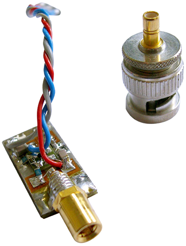 Figure 2. Prototype pocket-size white noise generator.
Low Power Zero-Drift Solution
Two design goals dominate this project:
Figure 2. Prototype pocket-size white noise generator.
Low Power Zero-Drift Solution
Two design goals dominate this project:
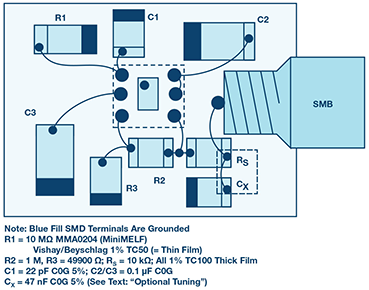 Figure 3. Gizmo layout.
Implementation Details
Loop area R1/C1/R3 should be minimized for best EMI rejection. Additionally, R1/C1 should be very well shielded from electrical fields, which will be discussed further in the EMI Considerations section. Although not critical, R1 should be shielded from large temperature changes. With good EMI shielding, thermal shielding is often adequate.
The LTC2063 rail-to-rail input voltage transition region of the VCM range should be avoided, as crossover may result in higher, less stable noise. For best results, use at least 1.1 V for V+ with the input at 0 common mode.
Note that RS of 10 kΩ may seem high, but the micropower LTC2063 presents a high output impedance; even 10 kΩ does not fully decouple the LTC2063 from load capacitance at its output. For this white noise generator circuit, some output capacitance that leads to peaking can be a design feature rather than a hazard.
The output sees 10 kΩ RS and a 50 nF CX to ground. This capacitor CX will interact with the LTC2063 circuit, resulting in some peaking in the frequency response. This peaking can be used to extend the flat bandwidth of the generator, in much the same way that port holes in loud speakers attempt to expand the low end. A high-Z load is assumed (>100 kΩ), as a lower-Z load would significantly reduce the output level, and may also affect peaking.
Figure 3. Gizmo layout.
Implementation Details
Loop area R1/C1/R3 should be minimized for best EMI rejection. Additionally, R1/C1 should be very well shielded from electrical fields, which will be discussed further in the EMI Considerations section. Although not critical, R1 should be shielded from large temperature changes. With good EMI shielding, thermal shielding is often adequate.
The LTC2063 rail-to-rail input voltage transition region of the VCM range should be avoided, as crossover may result in higher, less stable noise. For best results, use at least 1.1 V for V+ with the input at 0 common mode.
Note that RS of 10 kΩ may seem high, but the micropower LTC2063 presents a high output impedance; even 10 kΩ does not fully decouple the LTC2063 from load capacitance at its output. For this white noise generator circuit, some output capacitance that leads to peaking can be a design feature rather than a hazard.
The output sees 10 kΩ RS and a 50 nF CX to ground. This capacitor CX will interact with the LTC2063 circuit, resulting in some peaking in the frequency response. This peaking can be used to extend the flat bandwidth of the generator, in much the same way that port holes in loud speakers attempt to expand the low end. A high-Z load is assumed (>100 kΩ), as a lower-Z load would significantly reduce the output level, and may also affect peaking.
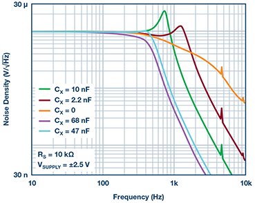 Figure 4. Output noise density of design in Figure 1.
Optional Tuning
Several IC parameters (for example, ROUT and GBW) affect flatness at the high frequency limit. Without access to a signal analyzer, the recommended value for CX is 47 nF, which typically yields 200 Hz to 300 Hz (–1 dB) bandwidth.
Nevertheless, CX can be optimized for either flatness or bandwidth, with CX = 30 nF to 50 nF typical. For wider bandwidth and more peaking, use a smaller CX. For a more damped response, use a larger CX.
Critical IC parameters are related to op amp supply current and parts with low supply current may require a somewhat larger CX, while parts with high supply current most likely require less than 30 nF while achieving wider flat bandwidth.
Plots shown here highlight how CX values affect closed-loop frequency response.
Figure 4. Output noise density of design in Figure 1.
Optional Tuning
Several IC parameters (for example, ROUT and GBW) affect flatness at the high frequency limit. Without access to a signal analyzer, the recommended value for CX is 47 nF, which typically yields 200 Hz to 300 Hz (–1 dB) bandwidth.
Nevertheless, CX can be optimized for either flatness or bandwidth, with CX = 30 nF to 50 nF typical. For wider bandwidth and more peaking, use a smaller CX. For a more damped response, use a larger CX.
Critical IC parameters are related to op amp supply current and parts with low supply current may require a somewhat larger CX, while parts with high supply current most likely require less than 30 nF while achieving wider flat bandwidth.
Plots shown here highlight how CX values affect closed-loop frequency response.
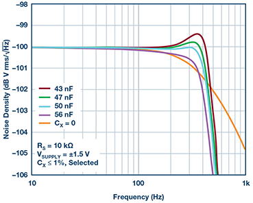 Figure 5. Zoomed in view of output noise density of design in Figure 1.
Measurements
Output noise density vs. CX (at RS = 10 kΩ, ±2.5 V supply) is reported in Figure 4. The output RC filter is effective in eliminating clock noise. The plot shows output vs. frequency for CX = 0 and CX = 2.2 nF/10 nF/47 nF/68 nF.
CX = 2.2 nF exhibits mild peaking, while peaking is strongest for CX = 10 nF, gradually decreasing for larger CX. The trace for CX = 68 nF shows no peaking, but has visibly lower flat bandwidth. The best result is for CX ~ 47 nF; clock noise is three orders of magnitude below signal level. Due to limited vertical resolution, it is impossible to judge with fine precision the flatness of output amplitude vs. frequency. This plot was produced using ±2.5 V battery supply, though the design allows the use of two coin cells (about ±1.5 V).
Figure 5 shows flatness magnified on the Y-axis. For many applications, flatness within 1 dB is enough to be useful and <0.5 dB is exemplary. Here, CX = 50 nF is best (RS = 10 kΩ, VSUPPLY ±1.5 V); CX = 45 nF, although 55 nF is acceptable.
High resolution flatness measurements take time; for this plot (10 Hz to 1 kHz, 1000 averages), about 20 minutes per trace. The standard solution uses CX = 50 nF. The traces shown for 43 nF, 47 nF, and 56 nF, all CS < 0.1% tolerance, show a small but visible deviation from best flatness. The orange trace for CX = 0 was added to show that peaking increases flat bandwidth (for Δ = 0.5 dB, from 230 Hz to 380 Hz).
2× 0.1 µF C0G in series is probably the simplest solution for an accurate 50 nF. 0.1 µF C0G 5% 1206 is easy to procure from Murata, TDK, and Kemet. Another option is a 47 nF C0G (1206 or 0805); this part is smaller, but may not be as commonly available. As stated prior, optimum CX varies with actual IC parameters.
Flatness was also checked vs. supply voltage; see Figure 6. The standard circuit is ±1.5 V. Changing supply voltage to ±1.0 V or ±2.5 V shows a small change in peaking as well as a small change in the flat level (due to VN changing vs. supply, with thermal noise dominant). Both peaking and flat level change ~0.2 dB over the full range of supply voltage. The plot suggests good amplitude stability and flatness when the circuit is powered from two small batteries.
Figure 5. Zoomed in view of output noise density of design in Figure 1.
Measurements
Output noise density vs. CX (at RS = 10 kΩ, ±2.5 V supply) is reported in Figure 4. The output RC filter is effective in eliminating clock noise. The plot shows output vs. frequency for CX = 0 and CX = 2.2 nF/10 nF/47 nF/68 nF.
CX = 2.2 nF exhibits mild peaking, while peaking is strongest for CX = 10 nF, gradually decreasing for larger CX. The trace for CX = 68 nF shows no peaking, but has visibly lower flat bandwidth. The best result is for CX ~ 47 nF; clock noise is three orders of magnitude below signal level. Due to limited vertical resolution, it is impossible to judge with fine precision the flatness of output amplitude vs. frequency. This plot was produced using ±2.5 V battery supply, though the design allows the use of two coin cells (about ±1.5 V).
Figure 5 shows flatness magnified on the Y-axis. For many applications, flatness within 1 dB is enough to be useful and <0.5 dB is exemplary. Here, CX = 50 nF is best (RS = 10 kΩ, VSUPPLY ±1.5 V); CX = 45 nF, although 55 nF is acceptable.
High resolution flatness measurements take time; for this plot (10 Hz to 1 kHz, 1000 averages), about 20 minutes per trace. The standard solution uses CX = 50 nF. The traces shown for 43 nF, 47 nF, and 56 nF, all CS < 0.1% tolerance, show a small but visible deviation from best flatness. The orange trace for CX = 0 was added to show that peaking increases flat bandwidth (for Δ = 0.5 dB, from 230 Hz to 380 Hz).
2× 0.1 µF C0G in series is probably the simplest solution for an accurate 50 nF. 0.1 µF C0G 5% 1206 is easy to procure from Murata, TDK, and Kemet. Another option is a 47 nF C0G (1206 or 0805); this part is smaller, but may not be as commonly available. As stated prior, optimum CX varies with actual IC parameters.
Flatness was also checked vs. supply voltage; see Figure 6. The standard circuit is ±1.5 V. Changing supply voltage to ±1.0 V or ±2.5 V shows a small change in peaking as well as a small change in the flat level (due to VN changing vs. supply, with thermal noise dominant). Both peaking and flat level change ~0.2 dB over the full range of supply voltage. The plot suggests good amplitude stability and flatness when the circuit is powered from two small batteries.
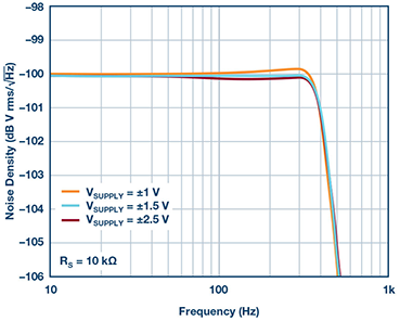 Figure 6. Output noise density for various supply voltages.
For this prototype at ±1.5 V supply, flatness was within 0.5 dB up to approximately 380 Hz. At ±1.0 V supply, flat level and peaking slightly increase. For ±1.5 V to ±2.5 V supply voltage, the output level does not visibly change. Total V p-p (or V rms) output level depends on the fixed 10 µV⁄√Hz density, as well as on bandwidth. For this prototype, the output signal is ~1.5 mV p-p. At some very low frequency (mHz range), noise density may increase beyond the specified 10 µV⁄√Hz. For this prototype it was verified that at 0.1 Hz, noise density is still flat at 10 µV⁄√Hz.
In stability vs. temperature, thermal noise dominates, so for T = 22(±6)°C, the amplitude change is ±1%, a change that would barely be visible on a plot.
EMI Considerations
The prototype uses a small copper foil with Kapton insulation as a shield. This foil, or flap, is wrapped around the input components (10 M + 22 pF), and soldered to ground on the PCB backside. Changing the position of the flap has significant effect on sensitivity to EMI and risk of low frequency (LF) spurs. Experimentation suggests that LF spurs that occasionally show are due to EMI, and that spurs can be prevented with very good shielding. With the flap, the prototype gives a clean response in the lab, without any additional mu-metal shielding. No mains noise or other spurs appear on a spectrum analyzer. If excess noise is visible on the signal, additional EMI shielding might be needed.
When an external power supply is used instead of batteries, common-mode current can easily add to the signal. It is recommended to connect the instrument grounds with a solid wire and use a CM choke in the supply wires to the generator.
Limitations
There are always applications that require more bandwidth, like full audio range or ultrasound range. More bandwidth is not realistic on a few µA of supply current. With approximately 300 Hz to 400 Hz of flat bandwidth, the LTC2063 resistor noise-based circuit could be useful to test some instruments for 50 Hz/60 Hz mains frequency, perhaps geophone applications. The range is suitable for testing various VLF applications (for example, sensor systems), as the frequency range extends down to <0.1 Hz.
The output signal level is low (<2 mV p-p). A follow-on LTC2063 configured as a noninverting amplifier with a gain of five and further RC output filter can provide a similarly well-controlled flat wideband noise output to 300 Hz with larger amplitude. In the case that does not maximize the closed-loop frequency range, a capacitor across the feedback resistor can lower the overall bandwidth. In this case, the effects of RS and CX will have less, or even negligible, effect at the edge of the closed-loop response.
Conclusion
The white noise generator described here is a small but essential tool. With long measurement times, the norm for LF applications—a simple, reliable, pocketable device that can produce near instantaneous circuit characterization—is a welcome addition to the engineer’s toolbox. Unlike complex instruments with numerous settings, this generator requires no user manual. This particular design features low supply current, essential for battery-powered operation in long duration VLF application measurements. When supply current is very low, there is no need for on/off switches. A generator that works on batteries also prevents common-mode currents.
The LTC2063 low power, zero-drift op amp used in this design is the key to meeting the constraints of the project. Its features enable use of a noise generating resistor gained up by a simple noninverting op amp circuit.
Figure 6. Output noise density for various supply voltages.
For this prototype at ±1.5 V supply, flatness was within 0.5 dB up to approximately 380 Hz. At ±1.0 V supply, flat level and peaking slightly increase. For ±1.5 V to ±2.5 V supply voltage, the output level does not visibly change. Total V p-p (or V rms) output level depends on the fixed 10 µV⁄√Hz density, as well as on bandwidth. For this prototype, the output signal is ~1.5 mV p-p. At some very low frequency (mHz range), noise density may increase beyond the specified 10 µV⁄√Hz. For this prototype it was verified that at 0.1 Hz, noise density is still flat at 10 µV⁄√Hz.
In stability vs. temperature, thermal noise dominates, so for T = 22(±6)°C, the amplitude change is ±1%, a change that would barely be visible on a plot.
EMI Considerations
The prototype uses a small copper foil with Kapton insulation as a shield. This foil, or flap, is wrapped around the input components (10 M + 22 pF), and soldered to ground on the PCB backside. Changing the position of the flap has significant effect on sensitivity to EMI and risk of low frequency (LF) spurs. Experimentation suggests that LF spurs that occasionally show are due to EMI, and that spurs can be prevented with very good shielding. With the flap, the prototype gives a clean response in the lab, without any additional mu-metal shielding. No mains noise or other spurs appear on a spectrum analyzer. If excess noise is visible on the signal, additional EMI shielding might be needed.
When an external power supply is used instead of batteries, common-mode current can easily add to the signal. It is recommended to connect the instrument grounds with a solid wire and use a CM choke in the supply wires to the generator.
Limitations
There are always applications that require more bandwidth, like full audio range or ultrasound range. More bandwidth is not realistic on a few µA of supply current. With approximately 300 Hz to 400 Hz of flat bandwidth, the LTC2063 resistor noise-based circuit could be useful to test some instruments for 50 Hz/60 Hz mains frequency, perhaps geophone applications. The range is suitable for testing various VLF applications (for example, sensor systems), as the frequency range extends down to <0.1 Hz.
The output signal level is low (<2 mV p-p). A follow-on LTC2063 configured as a noninverting amplifier with a gain of five and further RC output filter can provide a similarly well-controlled flat wideband noise output to 300 Hz with larger amplitude. In the case that does not maximize the closed-loop frequency range, a capacitor across the feedback resistor can lower the overall bandwidth. In this case, the effects of RS and CX will have less, or even negligible, effect at the edge of the closed-loop response.
Conclusion
The white noise generator described here is a small but essential tool. With long measurement times, the norm for LF applications—a simple, reliable, pocketable device that can produce near instantaneous circuit characterization—is a welcome addition to the engineer’s toolbox. Unlike complex instruments with numerous settings, this generator requires no user manual. This particular design features low supply current, essential for battery-powered operation in long duration VLF application measurements. When supply current is very low, there is no need for on/off switches. A generator that works on batteries also prevents common-mode currents.
The LTC2063 low power, zero-drift op amp used in this design is the key to meeting the constraints of the project. Its features enable use of a noise generating resistor gained up by a simple noninverting op amp circuit.
Authors:Aaron Schultz is an applications engineering manager in the LPS business unit at © Analog Devices Inc.. His multiple system engineering roles in both design and applications have exposed him to topics ranging across battery management, photovoltaics, dimmable LED drive circuits, low voltage and high current dc-to-dc conversion, high speed fiber optic communication, advanced DDR3 memory R&D, custom tool development, validation, and basic analog circuits, while over half of his career has been spent in power conversion. He graduated from Carnegie Mellon University in 1993 and MIT in 1995. Peter started in electronic development in 1986. Since 1993 he has worked as an independent consultant specializing in sensors and instrumentation. He has worked with many different customers, from small enterprises to large companies and scientific institutions. Peter lives in the center of 's-Hertogenbosch in the Netherlands next to St. Jan cathedral and shares his apartment with seven HP3562A signal analyzers.
| Resistor | Noise Voltage Density |
| 10 Ω | 0.402 nV/√Hz[/center] |
| 100 Ω | 1.27 nV/√Hz |
| 1 k Ω | 4.02 nV/√Hz |
| 10 kΩ | 12.7 nV/√Hz |
| 100 kΩ | 40.2 nV/√Hz |
| 1 MΩ | 127 nV/√Hz |
| 10 MΩ | 402 nV/√Hz |
Figure 1. Full schematic of white noise generator. Low drift micropower LTC2063 amplifies the Johnson noise of R1.
Consider Figure 1: a 10 MΩ resistor R1 generates white, Gaussian noise at the positive terminal of an op amp. Resistors R2 and R3 gain the noise voltage to the output. Capacitor C1 filters out chopper amplifier charge glitches. Output is a 10 µV/√Hz white noise signal.
Gain (1 + R2/R3) is high, 21 V/V in this example.
Even if R2 is high (1 MΩ), the noise from R2 compared to the gained up R1 noise is inconsequential.
An amplifier for the circuit must have sufficiently low input-referred voltage noise so as to let R1 dominate as the noise source. The reason: the resistor noise should dominate the overall accuracy of the circuit, not the amplifier. An amplifier for the circuit must have sufficiently low input-referred current noise to avoid (IN × R2) to approach (R1 noise × gain) for the same reason.
How Much Amplifier Voltage Noise Is Acceptable in the White Noise Generator?
Table 2 shows the increase in noise from adding independent sources. A change from 402 nV⁄√Hz to 502 nV⁄√Hz is only 1.9 dB in log volts, or 0.96 power dB. With op amp noise ~50% of the resistor noise, a 5% uncertainty in op amp VNOISE changes the output noise density by only 1%.
Table 2. Contribution of Op Amp Noise
| RNOISE (nV/√Hz) | Amp en | Total Input Referred |
| 402 nV/√Hz | 300 | 501.6 nV/√Hz |
| 402 nV/√Hz | 250 | 473.4 nV/√Hz |
| 402 nV/√Hz | 200 | 449.0 nV/√Hz |
| 402 nV/√Hz | 150 | 429.1 nV/√Hz |
| 402 nV/√Hz | 100 | 414.3 nV/√Hz |
Figure 2. Prototype pocket-size white noise generator.
Low Power Zero-Drift Solution
Two design goals dominate this project:
- An easy to use white noise generator must be portable; that is, battery-powered, which means micropower electronics.
- The generator must provide uniform noise output even at low frequencies—below 0.1 Hz and beyond.
Figure 3. Gizmo layout.
Implementation Details
Loop area R1/C1/R3 should be minimized for best EMI rejection. Additionally, R1/C1 should be very well shielded from electrical fields, which will be discussed further in the EMI Considerations section. Although not critical, R1 should be shielded from large temperature changes. With good EMI shielding, thermal shielding is often adequate.
The LTC2063 rail-to-rail input voltage transition region of the VCM range should be avoided, as crossover may result in higher, less stable noise. For best results, use at least 1.1 V for V+ with the input at 0 common mode.
Note that RS of 10 kΩ may seem high, but the micropower LTC2063 presents a high output impedance; even 10 kΩ does not fully decouple the LTC2063 from load capacitance at its output. For this white noise generator circuit, some output capacitance that leads to peaking can be a design feature rather than a hazard.
The output sees 10 kΩ RS and a 50 nF CX to ground. This capacitor CX will interact with the LTC2063 circuit, resulting in some peaking in the frequency response. This peaking can be used to extend the flat bandwidth of the generator, in much the same way that port holes in loud speakers attempt to expand the low end. A high-Z load is assumed (>100 kΩ), as a lower-Z load would significantly reduce the output level, and may also affect peaking.
Figure 4. Output noise density of design in Figure 1.
Optional Tuning
Several IC parameters (for example, ROUT and GBW) affect flatness at the high frequency limit. Without access to a signal analyzer, the recommended value for CX is 47 nF, which typically yields 200 Hz to 300 Hz (–1 dB) bandwidth.
Nevertheless, CX can be optimized for either flatness or bandwidth, with CX = 30 nF to 50 nF typical. For wider bandwidth and more peaking, use a smaller CX. For a more damped response, use a larger CX.
Critical IC parameters are related to op amp supply current and parts with low supply current may require a somewhat larger CX, while parts with high supply current most likely require less than 30 nF while achieving wider flat bandwidth.
Plots shown here highlight how CX values affect closed-loop frequency response.
Figure 5. Zoomed in view of output noise density of design in Figure 1.
Measurements
Output noise density vs. CX (at RS = 10 kΩ, ±2.5 V supply) is reported in Figure 4. The output RC filter is effective in eliminating clock noise. The plot shows output vs. frequency for CX = 0 and CX = 2.2 nF/10 nF/47 nF/68 nF.
CX = 2.2 nF exhibits mild peaking, while peaking is strongest for CX = 10 nF, gradually decreasing for larger CX. The trace for CX = 68 nF shows no peaking, but has visibly lower flat bandwidth. The best result is for CX ~ 47 nF; clock noise is three orders of magnitude below signal level. Due to limited vertical resolution, it is impossible to judge with fine precision the flatness of output amplitude vs. frequency. This plot was produced using ±2.5 V battery supply, though the design allows the use of two coin cells (about ±1.5 V).
Figure 5 shows flatness magnified on the Y-axis. For many applications, flatness within 1 dB is enough to be useful and <0.5 dB is exemplary. Here, CX = 50 nF is best (RS = 10 kΩ, VSUPPLY ±1.5 V); CX = 45 nF, although 55 nF is acceptable.
High resolution flatness measurements take time; for this plot (10 Hz to 1 kHz, 1000 averages), about 20 minutes per trace. The standard solution uses CX = 50 nF. The traces shown for 43 nF, 47 nF, and 56 nF, all CS < 0.1% tolerance, show a small but visible deviation from best flatness. The orange trace for CX = 0 was added to show that peaking increases flat bandwidth (for Δ = 0.5 dB, from 230 Hz to 380 Hz).
2× 0.1 µF C0G in series is probably the simplest solution for an accurate 50 nF. 0.1 µF C0G 5% 1206 is easy to procure from Murata, TDK, and Kemet. Another option is a 47 nF C0G (1206 or 0805); this part is smaller, but may not be as commonly available. As stated prior, optimum CX varies with actual IC parameters.
Flatness was also checked vs. supply voltage; see Figure 6. The standard circuit is ±1.5 V. Changing supply voltage to ±1.0 V or ±2.5 V shows a small change in peaking as well as a small change in the flat level (due to VN changing vs. supply, with thermal noise dominant). Both peaking and flat level change ~0.2 dB over the full range of supply voltage. The plot suggests good amplitude stability and flatness when the circuit is powered from two small batteries.
Figure 6. Output noise density for various supply voltages.
For this prototype at ±1.5 V supply, flatness was within 0.5 dB up to approximately 380 Hz. At ±1.0 V supply, flat level and peaking slightly increase. For ±1.5 V to ±2.5 V supply voltage, the output level does not visibly change. Total V p-p (or V rms) output level depends on the fixed 10 µV⁄√Hz density, as well as on bandwidth. For this prototype, the output signal is ~1.5 mV p-p. At some very low frequency (mHz range), noise density may increase beyond the specified 10 µV⁄√Hz. For this prototype it was verified that at 0.1 Hz, noise density is still flat at 10 µV⁄√Hz.
In stability vs. temperature, thermal noise dominates, so for T = 22(±6)°C, the amplitude change is ±1%, a change that would barely be visible on a plot.
EMI Considerations
The prototype uses a small copper foil with Kapton insulation as a shield. This foil, or flap, is wrapped around the input components (10 M + 22 pF), and soldered to ground on the PCB backside. Changing the position of the flap has significant effect on sensitivity to EMI and risk of low frequency (LF) spurs. Experimentation suggests that LF spurs that occasionally show are due to EMI, and that spurs can be prevented with very good shielding. With the flap, the prototype gives a clean response in the lab, without any additional mu-metal shielding. No mains noise or other spurs appear on a spectrum analyzer. If excess noise is visible on the signal, additional EMI shielding might be needed.
When an external power supply is used instead of batteries, common-mode current can easily add to the signal. It is recommended to connect the instrument grounds with a solid wire and use a CM choke in the supply wires to the generator.
Limitations
There are always applications that require more bandwidth, like full audio range or ultrasound range. More bandwidth is not realistic on a few µA of supply current. With approximately 300 Hz to 400 Hz of flat bandwidth, the LTC2063 resistor noise-based circuit could be useful to test some instruments for 50 Hz/60 Hz mains frequency, perhaps geophone applications. The range is suitable for testing various VLF applications (for example, sensor systems), as the frequency range extends down to <0.1 Hz.
The output signal level is low (<2 mV p-p). A follow-on LTC2063 configured as a noninverting amplifier with a gain of five and further RC output filter can provide a similarly well-controlled flat wideband noise output to 300 Hz with larger amplitude. In the case that does not maximize the closed-loop frequency range, a capacitor across the feedback resistor can lower the overall bandwidth. In this case, the effects of RS and CX will have less, or even negligible, effect at the edge of the closed-loop response.
Conclusion
The white noise generator described here is a small but essential tool. With long measurement times, the norm for LF applications—a simple, reliable, pocketable device that can produce near instantaneous circuit characterization—is a welcome addition to the engineer’s toolbox. Unlike complex instruments with numerous settings, this generator requires no user manual. This particular design features low supply current, essential for battery-powered operation in long duration VLF application measurements. When supply current is very low, there is no need for on/off switches. A generator that works on batteries also prevents common-mode currents.
The LTC2063 low power, zero-drift op amp used in this design is the key to meeting the constraints of the project. Its features enable use of a noise generating resistor gained up by a simple noninverting op amp circuit.Authors:Aaron Schultz is an applications engineering manager in the LPS business unit at © Analog Devices Inc.. His multiple system engineering roles in both design and applications have exposed him to topics ranging across battery management, photovoltaics, dimmable LED drive circuits, low voltage and high current dc-to-dc conversion, high speed fiber optic communication, advanced DDR3 memory R&D, custom tool development, validation, and basic analog circuits, while over half of his career has been spent in power conversion. He graduated from Carnegie Mellon University in 1993 and MIT in 1995. Peter started in electronic development in 1986. Since 1993 he has worked as an independent consultant specializing in sensors and instrumentation. He has worked with many different customers, from small enterprises to large companies and scientific institutions. Peter lives in the center of 's-Hertogenbosch in the Netherlands next to St. Jan cathedral and shares his apartment with seven HP3562A signal analyzers.