
© ilya shahau dreamstime.com
Components |
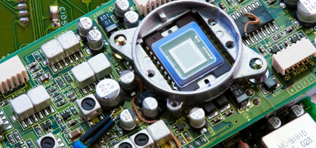
ASML and imec launch Advanced Patterning Center
ASML and imec announced the next major step in their extensive collaboration, with the launch of the Advanced Patterning Center.
Together they plan to tackle upcoming scaling challenges due to the chip industry’s move towards single digit nanometer dimensions. The Center will be located at the imec campus in Leuven and is expected to grow to close to 100 engineers over the next couple of years.
To guarantee critical dimension uniformity and overlay control, soon to be measured in fractions of one nanometer, imec and ASML will collaborate to investigate the practical interaction between all the different steps in the chip patterning process. The Advanced Patterning Center will use actual devices to analyse and optimize process steps as well as materials and device architecture choices, while applying integrated metrology.
The Advanced Patterning Center combines imec’s and ASML’s complementary expertise, engineering capabilities and patterning infrastructure to tackle these challenges, the infrastructure investments and the patterning knowledge requirements.
Imec will bring to the partnership its world leading clean room infrastructure (full 300mm pilot line with extension to 450mm) through which it supports a unique partner network of material and equipment suppliers, IDMs, foundries and fabless companies.
ASML will support the Advanced Patterning Center by making available its most advanced scanners, metrology systems and holistic lithography solutions, and by using the Center’s resources to optimize its offerings for the fab environment.
“ASML and imec have been partners for almost as long as both organizations exist, and while we have both benefited from this relationship, I believe the biggest beneficiary has been the chip industry which has gained faster access to breakthrough technology. I’m extremely confident that this continued investment in our joint capabilities will further accelerate technology development and new device introductions,” said Martin van den Brink, President and Chief Technology Officer at ASML.
“In order to stay ahead in today’s fast-evolving and equipment-intensive semiconductor business, it is critical that the entire semiconductor eco system has insight and access to state-of-the-art technology,” said Luc Van den hove, President and CEO at imec. “By bringing our collaboration to the next level, we will be able to expand our knowledge base more quickly and drive lithography advancements. In this way the global partner network of both companies will have access to the most advanced patterning processes for sub-10 nanometer technologies. This is crucial to better address future scaling and infrastructure challenges.”
