


© andrzej thiel dreamstime.com
Components |
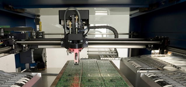
InnoLas Semiconductor on course for 450
Wafers with a diameter of 450 mm enable the Micro-chip industry an increase in yield of up to 80 percent.
‘This leads to an enormous increase in productivity. In order to control the product quality these wafers receive a specific marking from the manufacturer.
Promptly at the start of the year, InnoLas Semiconductor GmbH has successfully installed a second 450-mm system. As an optional Bridge-Tool variant the system can mark 450 mm and 300 mm wafers on either side. The system checks the result automatically and thus reduces the process operations significantly. According to requirements the customer can choose between vacuum handling and edge-grip handling. The latter transports the wafers especially carefully and cleanly.
The company places particular emphasis on in-house developments and products in the application of high-precision components. Together with the robust further development of proven engineering this takes care of the constant high quality standard in marking and handling processes, also for the new wafer sizes.
“The marking and handling quality will be maintained at our high level for the new wafer sizes. To achieve this we use components developed in-house whenever the requirements are of high precision. These are otherwise not available in suitable quality as required by us and our customers” Andreas Behr, General Manager of the InnoLas Semiconductor GmbH, explains the consistently high standard achieved by his wafer marking systems.