


© wizzyfx dreamstime.com
Components |
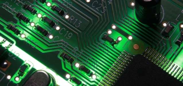
14nm FinFET test chip targeting Samsung process
ARM and Cadence tape out first 14nm FinFET test chip targeting Samsung process.
Designed with a complete Cadence RTL-to-signoff flow, the chip is the first to target Samsung's 14-nanometer FinFET process, accelerating the continuing move to high-density, high-performance and ultra-low power SoCs for future smartphones, tablets and all other advanced mobile devices.
In addition to the ARM Cortex-A7 processor, the test chip includes ARM Artisan standard-cell libraries, next-generation memories, and general purpose IOs. The test chip was designed using a complete Cadence RTL-to-signoff flow including Encounter® RTL Compiler, Encounter Test, Encounter Digital Implementation System, Cadence QRC Extraction, Encounter Timing System and Encounter Power System. This achievement is part of a systematic program to enable ARM technology-based SoCs on FinFET technology.
"Cadence's advanced node design flow, coupled with our collaboration with ARM and Samsung, is essential to semiconductor companies as they move to designing for a 14-nanometer FinFET process," said Dr. Chi-Ping Hsu, senior vice president, Research and Development, Silicon Realization Group at Cadence. "Our common goal is to enable our customers to reap the benefits and competitive advantages of designing at the most advanced technologies."
"End consumers are driving the need for better, faster, more connected devices," said Dr. Kyu-Myung Choi, senior vice president of System LSI infrastructure design center, Device Solutions, Samsung Electronics. "Our collaboration with ARM and Cadence allows us to innovate quickly as Samsung develops this new process technology for mobile multimedia applications."