


© Asus
Electronics Production |
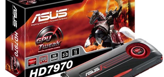
Inside the Asus AMD 7970 graphics card
Chipworks has found TSNS 28nm inside the Asus AMD 7970 graphics card.
There is no "Less is More" in the world of hard core gaming. High-end gamers "take glory in the fact that they can now play games like Metro 2033 at 85 frames-per-second (fps) when before they were limited to 78 fps".
No place for the faint-hearted
Some of guys that scored design wins; starting with some of the peripheral chips.
- Silicon Laboratories SL16010DC clock generator
- CHiL Semiconductor power management controller
- Fairchild NC7SZ74K8X MOSFET
- Fairchild FDMC8200 N-channel FET
- OnSemiconductor MC74VHCT125H MOSFET
- Coiltronics 1007R3-R15 inductors (6)
- OnSemiconductor MC78M05CDTG voltage regulator
- Programmable Microelectronics Corp Pm25LD010 serial flash memory
Surrounding the graphics chip are twelve 256 MB GDDR5 chips, for a total of 3 GB graphics RAM memory. The part number is the Hynix H5GQ2H24MFR GDDR5, which is a 2 Gb device rated at 6 GBps at 1.6 V. Twelve of them are used to give a 384 bit memory bus and memory bandwidth of 264 GB/s, writes Chipworks.
The AMD Radeon 7970 (Tahiti) is the first commercially available graphics processor fabricated at 28 nm by TSMC. Using the latest 28 nm technology lets AMD squeeze 2084 shaders, organized in 32 compute units, on to the die, for a total of 4.3 billion transistors in 365 sq. mm. The chip is clocked at 925 MHz, giving a theoretical performance of ~3.8 TFLOPS, compared with ~2.7 of the previous generation Radeon 6970.
Source: http://www.chipworks.com/