


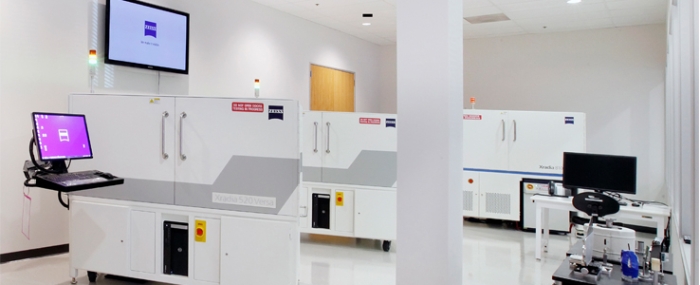
© zeiss
Business |
Zeiss enters the semiconductor process control market
Zeiss is fueling its growth strategy by expanding into a new market in the semiconductor industry.
Through its new Process Control Solutions (PCS) business unit, the company aims to leverage its core technology solutions and partnerships to address a range of special needs for semiconductor customers. The new business unit will be part of the Zeiss Semiconductor Manufacturing Technology (SMT) business group and draw from its expertise in Microscopy.
“We see a strong trend in semiconductors toward complex 3D chip structures and new materials,” explained Dr. Karl Lamprecht, head of SMT business group. “As development cycles lengthen and R&D costs climb, the role of metrology changes. Our customers need effective process control solutions delivering integrated, actionable information that speeds time to problem resolution and time to production. Zeiss has the technology and expertise to fulfill these requirements.”
The PCS business unit will utilize and expand upon Zeiss’s existing portfolio of products, including its proprietary microscopy technologies, to penetrate the semiconductor lab and fab space. Key products to be deployed include Zeiss’s electron microscope products Zeiss Crossbeam and Zeiss MultiSEM (the latter of which incorporates the company’s multi-electron-beam technology), ion-beam microscope Zeiss ORION NanoFab, as well as the Zeiss Xradia Versa and Zeiss Xradia Ultra non-destructive 3D X-ray microscope systems.
“Our process control solutions offer comprehensive structural, chemical and electrical information. By creating a single window into Zeiss for our semiconductor customers, we will enable them to address their process control challenges with seamlessly integrated technologies, helping them get their products to market faster,” said Dr. Raj Jammy, Head of Zeiss PCS business unit, headquartered in Pleasanton, California.
