
© alexander podshivalov dreamstime.com
Application Notes |
Fidelity Testing for A→D Converters
The ability to faithfully digitize a sine wave is a sensitive test of high resolution A→D converter fidelity. This application note (AN 132) was written by Jim Williams and Guy Hoover.
Introduction
The ability to faithfully digitize a sine wave is a sensitive test of high resolution A→D converter fidelity. This test requires a sine wave generator with residual distortion products approaching one part-per-million. Additionally, a computer-based A→D output monitor is necessary to read and display converter output spectral components. Performing this testing at reasonable cost and complexity requires construction of its elements and performance verification prior to use.
 Overview
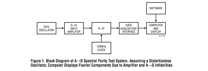
Figure 1 diagrams the system. A low distortion oscillator drives the A→D via an amplifier. The A→D output interface formats converter output and communicates with the computer which executes the spectral analysis software and displays the resulting data.
Overview
Figure 1 diagrams the system. A low distortion oscillator drives the A→D via an amplifier. The A→D output interface formats converter output and communicates with the computer which executes the spectral analysis software and displays the resulting data.
Overview
Figure 1 diagrams the system. A low distortion oscillator drives the A→D via an amplifier. The A→D output interface formats converter output and communicates with the computer which executes the spectral analysis software and displays the resulting data.
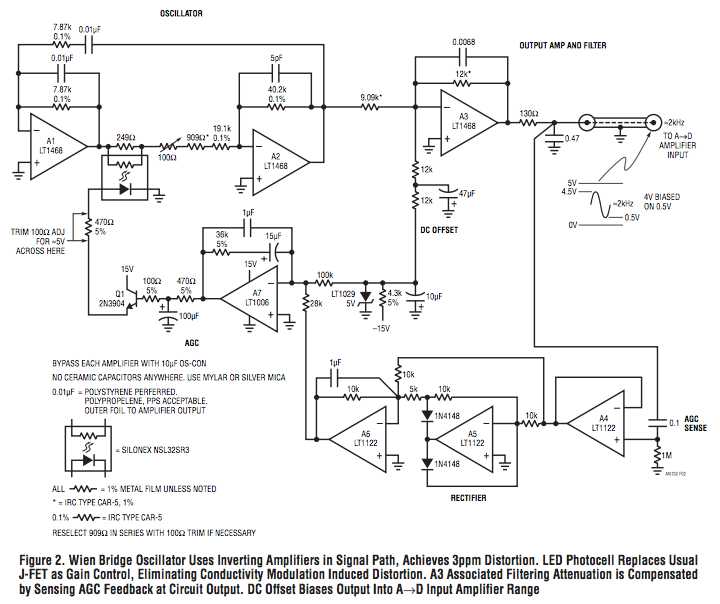
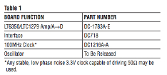
Oscillator Circuitry The oscillator is the system’s most difficult circuit design aspect. To meaningfully test 18-bit A→Ds, the oscillator must have transcendentally low levels of impurity, and these characteristics must be verified by independent means. Figure 2 is basically an “all inverting” 2kHz Wien bridge design (A1-A2) adapted from work by Winfield Hill of Harvard University. The original designs J-FET gain control is replaced with a LED driven CdS photocell isolator, eliminating J-FET conductivity modulation introduced errors and the trim required to minimize them. Band limited A3 receives A2 output and DC offset bias, providing output via a 2.6 KHz filter which drives the A→D input amplifier. Automatic gain control (AGC) for the A1-A2 oscillator is taken from the circuit output (“AGC sense”) by AC-coupled A4 which feeds rectifier A5-A6. A6’s DC output represents the AC amplitude of the circuit output sine wave. This value is balanced against the LT1029 reference by current summing resistors which terminate into AGC amplifier A7. A7, driving Q1, closes a gain control loop by setting LED current, and hence CdS cell resistance, to stabilize oscillator output amplitude. Deriving gain control feedback from the circuit’s output maintains output amplitude despite the attenuating band-limiting response of A3 and the output filter. It also places demands on A7 loop closure dynamics. Specifically, A3’s band limiting combines with the output filter, A6’s lag and ripple reduction components in Q1’s base to generate significant phase delay. A 1μF dominant pole at A7 along with an RC zero accommodates the delay, achieving stable loop compensation. This approach replaces closely tuned high order output filters with simple RC roll-offs, minimizing distortion while maintaining output amplitude. Eliminating oscillator related components from the LED bias is essential to maintaining low distortion. Any such residue will amplitude modulate the oscillator, introducing impure components. The band-limited AGC signal forward path is well filtered and the heavy RC time constant in Q1’s base provides a final, steep roll-off. Figure 3, Q1’s emitter current, shows about 1nA of oscillator related ripple out of a 10mA total, less than 0.1ppm The oscillator achieves its performance using only a single trim. This adjustment, which centers AGC capture range, is set in accordance with the schematic note. Verifying Oscillator Distortion Verifying oscillator distortion necessitates sophisticated measurement techniques. Attempts to measure distortion with a conventional distortion analyzer, even a high grade type, encounter limitations. Figure 4 shows oscillator output (Trace A) and its indicated distortion residuals at the analyzer output (Trace B). Oscillator related activity is faintly outlined in the analyzer noise and uncertainty floor. The HP-339A employed specifies a minimum measurable distortion of 18ppm; this photograph was taken with the instrument indicating 9ppm. This is beyond specification, and highly suspect, because of the pronounced uncertainties introduced when measuring distortion at or near equipment limits. Specialized analyzers with exquisitely low uncertainty floors are needed to meaningfully measure oscillator distortion. The Audio Precision 2722, specified at a 2.5ppm Total Harmonic Distortion + Noise (THD + N) limit (1.5ppm typical), supplied Figure 5’s data. This figure indicates a Total Harmonic Distortion (THD) of –110dB, or about 3ppm. Figure 6, taken with the same instrument, shows THD + N of 105dB, or about 5.8ppm. In Figure 7’s final test, the analyzer determines the oscillator’s spectral components with the third harmonic dominating at –112dB, or about 2.4ppm. These measurements provide confidence in applying the oscillator to A→D fidelity characterization. A→D Testing A→D testing routes oscillator output to the A→D via its input amplifier. The test measures distortion products produced by the input amplifier/A→D combination. A→D output is examined by the computer, which quantitatively indicates spectral error components in Figure 8’s display. The display includes time domain information showing the biased sine wave centered into the converter’s operating range, a Fourier transform indicating spectral error components and detailed tabulated readings. The LTC2379 18-Bit A→D/LT6350 amplifier combination under test produces 2nd harmonic distortion of –111dB, about 2.8ppm, with higher frequency harmonics well below this level. This indicates the A→D and its input amplifier are operating properly and within specifications. Possible harmonic cancellation between the oscillator and amplifier/A→D mandates testing several amplifier/A→D samples to enhance measurement confidence. APPENDIX A Tools for A→D Fidelity Testing; Circuit boards for implementing the text’s A→D testing are available. Table 1 lists the board functions and their part numbers. The computer software, PScope, is also available from © Linear Technology and may be downloaded at www.linear.com.-----
-----
-----
-----
-----
-----
-----