© Infineon
Components |
Smart and Small: New Infineon 3D image sensor chip family
Infineon Technologies AG introduced a family of 3D Image Sensor chips for implementation of touchless gesture recognition.
Developed in cooperation with pmdtechnologies GmbH, the new chips are the first to combine a 3D image sensing pixel array with the digital conversion and control functionality needed to design very compact and accurate monocular systems for gesture recognition applications in computers and consumer electronics devices.
Touchless Gesture Control
The Infineon 3D Image Sensor chips will simplify and enhance the way people interact with machines. They enable fast and reliable tracking of finger movements and hand gestures to complement today’s touch screen and mouse or stylus user interfaces.
“Gesture recognition will dramatically change the way people control computing and consumer electronic systems,” says Ralf Bornefeld, Vice President and General Manager of the Sense & Control business line at Infineon Technologies AG. “We expect touchless gesture interfaces based on our 3D Image Sensor to change the user experience and enhance productivity the same way that the mouse did decades ago with the PC.”
3D cameras based on the Infineon 3D Image Sensor chip family can achieve unmatched levels of miniaturization and deliver an excellent user experience. High level integration lowers cost and size of a complete camera module. In fact, a reference design based on this chip is the smallest 3D image sensing camera now available.
Collaboration with pmdtechnologies
The Infineon 3D Image Sensor chips were developed in collaboration with pmdtechnologies GmbH (Siegen, Germany), which is recognized as the world’s leading technology provider for 3D Image Sensors based on the Time-of-Flight (ToF) principle. The new chip family includes pmd’s ToF pixel matrix and patented Suppression of Background Illumination (SBI), a feature which improves the sensor chip’s dynamic range for indoor and outdoor operations.
"The consolidation of the existing and mature Time-of-Flight 3D sensing know-how at pmd and the volume-proven, mixed-signal CMOS process technology and design expertise of Infineon will pave the way to the best possible user experience for touchless gesture recognition applications,” says Dr. Bernd Buxbaum, CEO of pmdtechnologies.
Key Features of the Infineon 3D Image Sensor Family
The Infineon chip family offers the highest level of integration now available, including the photosensitive pixel array, sophisticated control logic, digital interfaces with ADCs (Analog-to-Digital Converters) and digital outputs.
The Infineon 3D Image Sensor family currently includes two members. The IRS1010C has a resolution of 160x120 pixels and the IRS1020C has a resolution of 352x288 pixels. Both are dynamically configurable via I²C interface, allowing adjustment in real time to changing lighting and operating conditions. The chips are delivered as bare die for integration with camera lens and Infra-Red (IR) illumination source in a camera module.
Availability of 3D Image Sensors, camera reference design and starter kits
Samples of the Infineon 3D Image Sensors are now available for development of 3D camera systems. Volume production is planned for mid-2014.
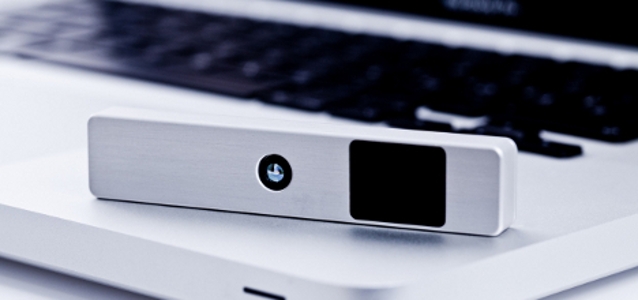
Also available is the CamBoard pico, the world’s smallest reference design for 3D cameras. Designed by pmdtechnologies, this USB-powered QQVGA resolution 3D camera is based on the IRS1010C 3D Image Sensor chip. It measures only 85 x 17 x 8 mm³, which makes it the smallest depth sensing camera available today.
The CamBoard pico demonstrates the extremely low latency and precision achieved with the Infineon 3D Image Sensor chip, which are the key enabling factors for touchless gesture interaction.


