
© iFixit
Business |
Apple A6 processor teardown
The stuff you'll see in the Apple A6 teardown is the kind of thing that's usually done behind closed doors, in some super-secret facility buried six miles beneath the Earth's surface. But not today.
Today, Chipworks has agreed to let the common nerd (us!) into their lab and show off some of their high-tech gizmos—all the while delving deeper into Apple's A6 processor and other chips we discovered in last week's iPhone 5 teardown.
This time there's no repairability score; it's all fun and games. Join us in our journey of discovery... through science!
Highlights: Chipworks has a bona-fide ion blaster, affectionately called Ibe (short for "ion beam etching"). Ibe is used to remove layers of semiconductor devices in a controlled and selective manner with very precise and planar results. Think of ion beam etching as being akin to sandblasting a chip to remove specific layers. Instead of sand, though, Ibe uses the atoms in an ion beam to do its dirty work. Ions, man... ions. So how were the A6 photos created, you ask?© iFixit
- The A6 is first decapsulated in a fuming sulfuric acid solution, heated to a temperature designed to get best results.
- Then, Chipworks engineers use a microscope to take images of the die. The die is loaded onto a servo-controlled X-Y table, and focus is set and maintained by laser monitoring.
- Image coordinates are programmed into the system. The microscope moves the die automatically and takes several images, which are stitched together to create the full die photo.
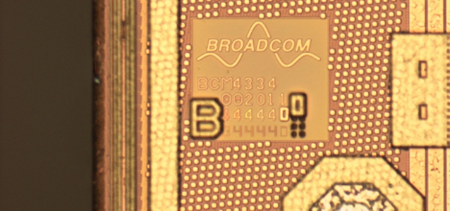
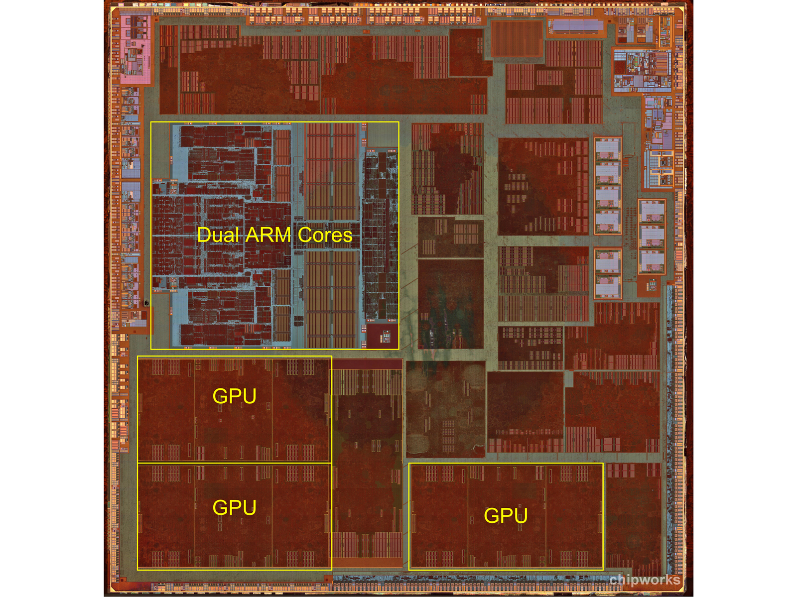
Delving deeper into the center of the A6, we find dual ARM cores and three PowerVR graphics cores! Generally speaking, logic blocks—such as those found in the A6—are automagically laid out with the use of advanced computer software. However, it looks like the ARM core blocks were laid out manually—as in, *by hand*. A manual layout will usually result in faster processing speeds, but it is much more expensive and time consuming. The manual layout of the ARM processors lends much credence to the rumor that Apple designed a custom processor of the same caliber as the all-new Cortex-A15. It just might be the only manual layout in a chip to hit the market in several years. Chipworks cracked open the Apple 338S1077 to confirm that it is, in fact, a Cirrus CS35L19 class-D audio amplifier—and not an audio codec as initially thought. The Murata Wi-Fi SoC module is actually comprised of a Broadcom BCM4334 package in addition to an oscillator, capacitors, resistors, etc. Murata assembles all of the components together and sends their package to Foxconn, where it eventually ends up on the iPhone's logic board. Chipworks said it best: "Murata makes a house that is full of other people's furniture." The Broadcom BCM4334, fabricated in Taiwan at TSMC on a 40 nm CMOS process, features:© iFixit
- Wi-Fi (802.11 a/b/g/n)
- Bluetooth 4.0 + HS
- FM Receiver