
© LWC
Business |
Applied Materials & IME with joint R&D centre
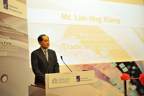
Applied Materials, Inc. and the Institute of Microelectronics (IME) officially opened the Centre of Excellence in Advanced Packaging at Singapore’s Science Park II.
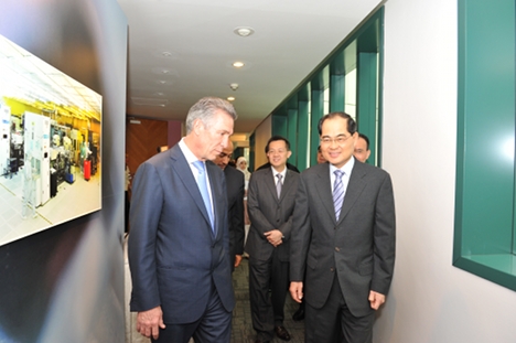
The Centre of Excellence in Advanced Packaging has been built with a combined investment of over USD$100 million from Applied Materials and IME. The world-class facility features a 14,000 square foot Class-10 cleanroom and is equipped with a fully-integrated line of 300 millimetre manufacturing systems to support the research and development of 3D chip packaging, a critical growth area for the semiconductor industry.
Traditionally, chips are connected to packages using wires attached to only their edges. This approach limits the possible number of connections from the chip and the long wire connections result in signal speed delays and power inefficiencies. With 3D chip packaging, multiple chips can be stacked on top of each other and connected with wiring that runs vertically through the stack – called through-silicon vias (TSVs). When used to stack memory chips on logic chips, this technology is expected to reduce package size by 35%, decrease power consumption by 50%, and increase data bandwidth by a factor of eight or more times.
Conceived to support research collaboration between Applied Materials and IME, the Centre will also allow both parties to pursue independent research initiatives including process engineering, integration and hardware development. For Applied Materials, this is a significant addition of new capabilities in Singapore. The Centre also serves as a demonstration of how A*STAR is able to develop and nurture a local ecosystem for advanced R&D through partnerships with leading corporations. Research activities are already underway with a team of over 50 personnel.
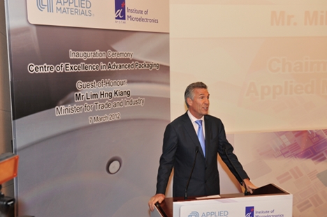
“Today, we are not only opening the most advanced wafer level packaging lab of its kind in the world, but we are also opening a new product development capability for Applied Materials in Asia,” said Mike Splinter, Chairman and Chief Executive Officer of Applied Materials. “This Centre will strengthen our ability to advance new technologies and allow us to work more closely with our customers in Asia.”
© LWC
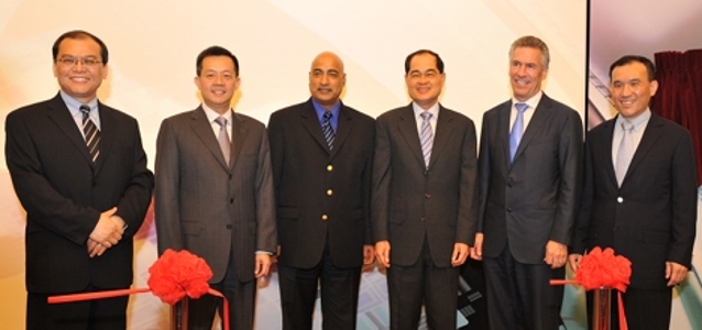
On the collaboration with Applied Materials, Mr. Lim Chuan Poh, Chairman of A*STAR, said, “The combined efforts of Applied Materials and A*STAR’s Institute of Microelectronics are a continuing testimony to A*STAR’s spectrum of excellent and industry-relevant scientific capabilities. It reaffirms our strategy of leveraging a suite of capabilities to form meaningful and impactful public-private research alliances which catalyse the growth of private sector R&D activities in Singapore. This will create many high-value jobs locally and help to further anchor Singapore’s semiconductor manufacturing base.”
Professor Dim-Lee Kwong, Executive Director of IME, added, “The Centre of Excellence is a prime example of a strategic relationship fostered between two leading players in the global semiconductor value chain and will spur the development of innovative wafer-level packaging technologies to be implemented globally. This collaboration will enable the semiconductor industry to accelerate the adoption of 3D chip packaging.”